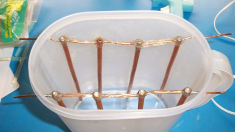
For the few double-sided PCBs we’ve actually etched at home we simply soldered a piece of wire to either side of a via and clipped off the excess. But if you want to go the extra mile you can’t beat electroplated through holes. The setup seen above is an electroplating tank build from simple materials which [Bearmos] has been working on.
The two sets of copper structures are both used as anodes. Some copper water pipe (like you’d use for a refrigerator ice maker) was cut into short rods and soldered onto pieces of bus wire. The portion of the metal which will stick above the chemical bath was coated with a generous layer of hot glue. This will protect it from corrosion cause by the off-gassing during the plating process. The traces of the etched PCB act as the anodes, but the holes themselves must be conductive in order for the plating process to work. A water proof glue with powdered graphite mixed in is applied to all of the holes in the substrate. This technique is based on the huge electroplating guide published by Think & Tinker.


“The traces of the etched PCB act as the anodes…”
According to the article, the PCB traces are the cathodes.
Copper ions are positively charged. To attract them to a surface that surfacem ust have a negative charge, since unlike charges attract. So the copper traces should be cathodes.
I’m trying to find more build details, as I kinda want to make one for our highschool, which has an etching room and several CNCs, but still has to stick little wires through PCBs in order to do vias.
jobgg, what other build details do you need to know – I thought I had included everything. There are 4 parts to he article, as well as more info on Think and Tinker(linked to in the HaD post and elsewhere).
What details are missing?
Nifty, but still looks like a pain in the ass. (Being a chemical process and whatnot.)
I finally gave in and bought a bottle of those copper through-hole rivets they sell on MegaUK. (Since I’m in the US, I had to order them via phone through VPC Inc.) Haven’t had an opportunity to use them yet though.
So I guess you have to drill holes first on virgin copper, do this activation and plating – THEN photo resist – artwork – expose (2 sides)- develop – etch. That means you will need your hole mask first and hope the artwork lines up properly later. Sounds doable, it beats how I make my thru-holes with tiny copper tubes I roll from foil.- tedious.
I will definitely give this a whirl.. Great project!
The process is:
Clean plates->drill holes->activate->electroplate->put in CNC->mill the traces
After the holes have been plated you can’t etch the board because you can’t mask the holes and they would be dissolved.
Had not though of that. Interesting.. humm..
Actually you can mask the holes with acrylic paint (just use a vacuum cleaner to suck the paint in the holes).
obviously you were using toner transfer. uv film is designed for “tent” operation. ie it covers said holes
This was originally intended to be used with a CNC PCB mill.
You can etch the boards (this is how the “real” PCB fab’s do it), but you’ll need another (intermediate) process tank for applying the etch resist to the PTH’s and copper (traces, etc) that you’ll want to keep. . .
So, the process in this case would be: drill holes->plate through holes->apply negative mask->apply etch resist->etch
This is only good for people that want to do it at home to see how it all works. Otherwise you will spend 10X what it costs to have a board made and it can be dangerous if you are not careful.
Still if you are capable and have the money it is worth doing to understand all the steps.
I have been making double sided pcb’s at home for years now, and got quite good at it. Mostly I find it fun and rewarding. (im nuts i know) And this is exactly what I have been looking for to further enhance my process. I would think it’s less expensive than getting it done out of house; never did so I don’t know. Not to mention you can make a board quickly.
even in 2017 people are still saying board making at home is dead…so i decided to look. 100x70mm min of 10mil trace 5 mil spacing… have to get 3 copies and it costs $111 for 1 or 2 week turn around. unless im missing something at home is cheaper once you have the stuff. I happened to have had a stack of plexi from when a friend worked at a hardware store and brought home the cut scraps they would have discarded. When you also have a miter saw and buy a 80 tooth blade from harbor freight and combind with the knowledge that acetone welds plexi… all the sudden your etch tank is cheap af. I built a dev box from plexi as well, adjustable y and z axis but fixed in center on x axis. single high efficency 365nm led. i see people talking about 18w no name china 390nm arrays and laugh cause most of the time my 35 buck single diode actually puts out more uv and in the wavelength the resist is looking for.
im constructing a high speed press from a brushless rc motor (1450w) and a linear slide rail. the motor has a 8mm shaft which i will swap wtih the cnc shank with colet on one end. people say the at home is dead but i think this is the perfect time. If all else fails ill start a hacker space in my town cause i will have everything required anyway
I use these special rivets:
http://smdshop.nl/product_info.php?cPath=47&products_id=146&language=en
They are cheap and supereasy to work with and you can still stick components through the holes. That’s epecially handy when you want to solder components that don’t allow you to solder on both sides of the board like header connectors.
Wow, I wonder if they ship internationally. My only option was to buy 1000 of them (One size!) from a US Mega Electronics distributor for ~$85 shipped. :|
I know that he sends internationally in Europe but I don’t know whether he send to the US. Sending a small package to the US from The Netherlands costs about 10euro.
Wow this is great.
I can see how the process is much easier with isolation milling rather than etching traces, but I always thought that isolation milling is a really cool way to make a one-off board prototype anyway so this works for me. It’s a good way to make one board to try your design and verify it’s right before sending it off to have multiple copies made if nothing else. Isn’t there always at least a couple errors or tweaks with a board design you would have liked to find before you ever ordered that alpha batch?
I have looked at the think & tinker conductive ink but the price is very high and not worth it unless you do a fair bit of this kind of thing, considering the shelf life and all.
So to me the eureka items are the dirt-cheap conductive ink and the probing routine for compensating for board height, which is tricky and not reliable with my mechanical methods for trying to just make things flat. The probing looks like it makes it dead easy !
Clever info to glean from your site. I for one am tickled that you have shouted it from the rooftops. I will definitely be trying your methods myself.
I’m glad you found it useful. if you read through the comments at the bottom of the article you’ll find that a few people have reported back with a fair amount of success when trying this themselves. There are a few “tricks” for the CNC portion as well specifically address PCB CNC optimizations:http://twilightrobotics.com/cnc/cncnot2
Also, cpirius has posted a youtube video that demonstrates the entire process start to finish:http://www.youtube.com/watch?v=yqjKohZX2t8