When a project starts off by heating acid to its boiling point we say no thanks. But then again we’re more for the projects that use ones and zeros or a hot soldering iron. If you’re comfortable with the chemistry like [Michail] this might be right up your alley. He used boiling acid to expose and photograph the die from several integrated circuits.
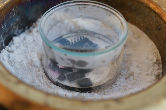
The title of our feature is a play on words. In this case, die refers to the silicone on which the IC has been etched. To protect it the hardware manufacturer first attaches the metal pins to the die, then encapsulates it in plastic. [Michail] removes that plastic case by heating sulfuric acid to about 300 degrees Celsius (that’s 572 Fahrenheit) then submerges the chips in the acid inside of a sealed container for about forty minutes. Some of the larger packages require multiple trips through the acid bath. After this he takes detailed pictures of the die and uses post processing to color enhance them.
This isn’t the only way to get to the guts of a chip. We’ve seen nitric acid and even tree sap (in the form of bow rosin) do the trick.


“Do you expect me to talk?”
“No Mr. Bondwire, I expect you to die!”
*clap*
*clap*
*clap*
(Actually pretty funny. I just haven’t used sarcastic clapping in a long time…)
Sorry, couldn’t resist the obligatory xkcd reference: http://xkcd.com/123/
silicone != silicon
My high school chemistry teacher always said silicone instead of silicon and it drove me nuts. The world needs an army of people like you.
Thanks for the compliment, but the world barely tolerates the one of me that already exists.
I had a health teacher that always said “prostrate” instead of “prostate”. That was almost as annoying except I was in Jr. High and it made everyone giggle.
IIRC I ruined his curve by pointing out on the final exam that three of the answers on his answer sheet were incorrect. :p
We are word nerds.
We are legion.
We do not forgive bad spelling, punctuation, or usage.
We do not forget what our English teachers taught us.
Expect us to be correct.
Failure shows a lack of education, unless it is not your primary language.
My _college_ Chemistry teacher as well!
extreme pin decapping :
http://www.zhigao5191.com/computer-network/tp-link740nv5luyouqiguauyinusbkou.html
https://forum.openwrt.org/viewtopic.php?id=37368
also a sweet hack in itself
Can somebody explain why the rosin dissolves the epoxy? Until now, I didn’t assume that rosin is an organic dissolving agent since I know that rosin itself is dissolved by another dissolving agent when used in contact glue.
Rosin is derived from pine trees (usually), and colophony is the term used for the rosin traditionally used for rosin core solder, and also rosin for stringed instruments. The word colophony comes from the ancient Greek city name Colophon where it was traditionally harvested. The choice of flux, resin based, organic or inorganic, depends on how aggressively you want to deoxidise and clean the items being bonded, the properties of the materials being bonded, and the temperatures being applied. Rosin core solder has natural acids that help to prepare the surfaces for soldering, but is not as aggressive as other available fluxes (“it’s just right”), hence it’s use in delicate electronics. If it weren’t a bit chemically aggressive, it wouldn’t be useful as a flux. Rosin is also a good way to flare up asthma.
That takes me back to my old colophon harvesting days…
It’s silicon, not silicone. Silicon goes in integrated circuits. Silicone goes in fake boobies.
Boobies? Not anymore, it’s dangerous, now the more common thing is to use bags of water I hear.
As others have stated, it is silicon, not silicone. Also, the die are not etched on the silicon. The silicon is doped to make the P’s and the N’s. The metal layers are etched.
Mike has made the silicon-silicone error before.
Also, I’d assume the etching process is implied, similar to someone saying you’re walking on the ground, when you’re actually walking on the floor, on the ground.
While I doubt the author knew this, there is actually etching involved. Silicon wafers go through a photoresist/etch process before doping – that’s how you get it doped in one spot and not another.
Not to mention that some of these devices may have poly-silicon trace layers which are etched.
Wow that’s a crazy amount of acid. If you want only a small section of the top of die opened up: Get a dremel with a grind tool, and grind down till you get to the die. If you see the die, congratulations, you’ve just damaged it. You want to get a feel for how far down the die is. Now get another of the same type of IC. Dremel down not quite so far. Have a little fuming nitric on hand (not boiling!) as well as (about a shot glass) of acetone. Of course, be careful if handling acid. Put the IC on a hot plate. You’ll only need a few DROPS of the fuming nitric acid, but use a glass dropper as it would eat through plastic. Heat is a catalyst for the nitric eating the plastic. Add a little fuming nitric to the crater you’ve dremeled out, with the IC sitting on the hot plate. After a few seconds of nitric acid + IC, dunk in acetone to rinse. Repeat the drop of nitric / wait 5 sec on hot plate / acetone rinse until you see bare die. By the time you’re done the device should still be functional, and you’ll be able to probe down on the die itself if you have some microprobes and can break thru the passivation layer. But lasers are a another discussion…
You almost have it. First off, Fuming nitric will not aggressively eat plastic. Plastic pipettes work great for Fuming Nitric. Sulfuric however will eat those plastic pipettes right quick and you should use a glass pipette. I don’t typically cut into the package mechanically unless it is very thick, though a little scoring will help the first few drops of acid stay right where you want. For the process your acid should be room temperature and you should only have a pipette of it out at a time (which is plenty for any package I have decapped)
My typical process is this,
-Heat the device on a hotplate (about 70 deg C. You’ll get a feel for your materials over time)
-Apply a drop of acid to the top of the package above the die and let it react for 1-2 seconds. You’ll see it eat at the mold compund.
-Remove the reacted material with a q-tip and if needed rinse with acetone. Distilled water can be used as well. You should only ever have a drop of acid on the package at a time
-Repeat these steps until the die is neatly exposed. With practice you can completely expose the die while leaving the chip in perfectly function condition allowing for all kinds of neat analysis. The process goes quicker with experience. Take it slow your first dozen or so tries and you’ll get good results. Once you get better you can expect to spend 2-5 minutes on a package.
Now a few notes about materials
Fuming Nitric is very aggressive on mold compounds used to encapsulate dies and will quickly have you a gooey mess if you aren’t careful. Sulfuric is a lot slower but will get you there. One thing to note is that Nitric will destroy copper extremely fast and a few devices, especially high power analog stuff, have copper traces above the top layer passivation. If you use straight nitric acid these traces will be gone the second the die is exposed, but you can prevent that by mixxing nitric and sulfuric 3:1. The sulfuric will act as a buffer for the copper and give you a few seconds of protection.
Try put fuming nitric acid on thermoplastic, it will smoke, melt and maybe catch on fire
Nice post! Yeah you’re right about the plastic pipette and nitric. It’s been a good 5 years or so since I’ve decapped a device, and now that I think about it, we did use plastic pipettes for the nitric. I work in the industry, and we have a group that does the failure analysis work for us, but on occasion we used to open them up to get a quick look and probe down on signals for a quick turn debug or just to check that the bonding was correct. Thanks for clarifying the bit about nitric going after copper. I meant to mention that. It will also react with the bond wires (my experience was with Gold wire, but Copper wire will be eaten away much quicker than Gold).
I’ve seen such approach, but why acetone? It does not dissolve plastic nor carbon…
The acetone is to clean the acid residue after it has reacted with the package, not to work on the package itself. I suspect that the reasons to use acetone are that it does not react violently with sulfuric acid like water does, it is a common solvent used in glass cleaning which is what your die’s outermost surface is, and it will not damage any of the materials that comprise a device. The real reason I used it though is because my chemist told me to and he is much more knowledgeable about it than me.
Many comments, and nobody mentioned how awesome these pictures are! Great work! (and really high-quality images). I guess I will print & hang the whole series on my kitchen wall, they are just too beautiful to rot in my Download folder…
Yes, certainly is excellent work.
I find it striking how irregular the main areas of the AVR devices look. With the random scattering of long vertical lines on a grid arrangement they could almost be “hardened” FPGA designs.
I wonder if they are. It would explain the large die size. Atmel make their own line of FPGAs don’t they?
Nope, they are not ‘hardened’ FPGA, it’s just autorouted standard cell logic synthesis.
No, they are not ‘hardened’ FPGA.
These areas are auto-routed “standard cell” logic.
Ah ok then. The profusion of parallel straight lines in the top metal layer had me wondering. Why are there so few bends visible though? Was it a really quick auto route job? Do Atmel chuck out a few dozen new designs at a time then reserve a tidy rev. B layout only for the ones that prove popular?
I know that I will dye one day.
What type of camera is used to take the pics? And/or is some additional prep work needed to get said pictures?
Photos are from metallographic microscope with 5Mp camera attachment. Usually 4-20 shots are taken and then stitched together into large photo.
The only image processing thing is some saturation adjustment in camera software.
Remember next time to breath in with your remaining good nostril if you’re not using a proper vent hood with this procedure.