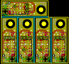
Some PCB production houses – Seeed Studio and itead studio, especially – allow you to upload a gerber file and receive a printed circuit board very inexpensively. The pricing structure for these board houses is based on predesignated board sizes – 5cm square or 5×10 cm – and sometimes a project is just too small to justify buying a full 25 square centimeters of board. This is where panelizing comes in: by putting multiple copies of a circuit board on one of the available sizes you can get more boards for the same amount of money. But how to panelize your boards without the (sometimes) hassle of cutting and pasting?
[Martin] came up with a way of panelizing PCBs with just a Python script. By creating one copy of a circuit board in KiCAD, he can fire up his script and tell the computer exactly how to duplicate his circuit to fit any size board.
By his own admission, [Martin]’s script is still a little clunky, but it does allow him to edit the panelized board in KiCAD and also copies the nets so the ratsnest doesn’t go between boards.


I just sent for a 5×5 cm board with 24 copies of the same design on it. It will be fun to see if Seeedstudio accepts it since they claim to only allow a maximum of 5 copies….
…either your boards are microscopic or you’re mistaking cm with inches :O
Well, 24 copies on 1 5x5cm board would put each board at a hair over 1cm^2. I can see some use in boards that size. Often a breakout board.
Mhm with a bit of margin… yeah i guess :)
Looking at his twitter feed, it seems reasonable
https://twitter.com/matseng/status/279973655377760256/photo/1
Yup, many really small breakout boards and some extra space at the top for two 2.5mm registration holes if I ever make a solderpaste stencil for it.
http://dangerousprototypes.com/forum/download/file.php?id=9315&mode=view
Does Seeed Studio makes the necessary v-scoring in order to depanelize?
Nah, both Seeed and iTead claim to only support silkscreen as your panel lines, and leave it up to you to depanelize on your own. No v-scoring, no routed sections with perforated tabs, no large drilled sections, etc. I’m not sure how many drills in a row you could get away with before they’d reject it outright.
I have a 3-up on a 5×5 panel I’m about ready to submit as soon as my current order is delivered and I validate the layout against reality. I totally bashed Eagle into it by making a blank board and copying a singleton instance onto it three times before renaming the common nets. (I figure that way if I do split them, they’re three independent boards, but if I leave them together, VCC and GND can power all 3 with one source without jumper wiring.) I half expect it’ll have something go horribly wrong, but that’s the price of learning sometimes.
“For the following services, you can panelize to save the cost, but you need to cut the board by yourself.” http://www.seeedstudio.com/depot/fusion-pcb-service-p-835.html
By selecting 0.8 mm thick board (at no extra cost from Seeed) it’s easy to snap the boards apart after scoring the boards with a knife. The standard 1.6 mm is not so easy unless you have a hacksaw, or even better, a wet saw for cutting tiles.
I usually put a 0.2mm wide rectangle on the tStop & bStop layers to get a small groove in the soldermask for easier cutting a straight line.
On one occasion I actually got the board vscored from Seeed by doing this – must have been a fluke in their processing. It was a 5×5 cm board with 9 copies sized 5mm x 50mm.
Manual panelization is supported in KiCAD. In PCBNew, goto File->Append Board to add a new (or the same) board to the current layout. There is a video tutorial of this here: http://www.youtube.com/watch?v=3qzL1APxtiU
Hello and thank you for your inputs to this thread. I’m using KiCad v5,00 and I need to create a 4 x 5 panel of 17mm x 37mm boards. I’m not seeing the File -> Append Board function you refer to. What version did you find this function in?Also, the YouTube video you reference is no longer available. If you have any updated information please let us know. Perry
You don’t see the menu because you are running pcbnew from within Kicad. You have to run pcbnew “stand-alone” rather than from within Kicad. The menu entries you desire will appear when running independently, but not when running as one integrated program. I’m not sure why. The schematic editor, eeschema, also shows different menu items when running alone than when running from within Kicad.