It’s time to do a series on logic including things such as programmable logic, state machines, and the lesser known demons such as switching hazards. It is best to start at the beginning — but even experts will enjoy this refresher and might even learn a trick or two. I’ll start with logic symbols, alternate symbols, small Boolean truth tables and some oddball things that we can do with basic logic. The narrative version is found in the video, with a full reference laid out in the rest of this post.
Invert
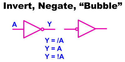 The most simple piece of logic is inversion; making a high change to low or a low change to high. Shown are a couple of ways to write an inversion including the ubiquitous “bubble” that we can apply almost anywhere to imply an inversion or a “True Low”. If it was a one it is now a zero, where it was a low it is now a high, and where it was true it is now untrue.
AND
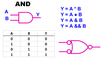 Moving on to the AND gate we see a simple truth table, also known as a Boolean Table, where it describes the function of “A AND B”. This is also our first opportunity to see the application of an alternate symbol. In this case a “low OR a low yields a low”
NAND
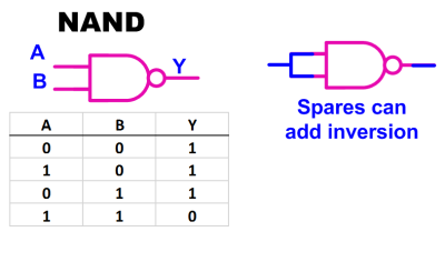 Most if not all of the standard logic blocks come in an inverted form also such as the NAND gate shown here. The ability to invert logic functions is so useful in real life that I probably used at least three times the number of NAND gates as regular AND gates when doing medium or larger system design. The useful inversion can occur as spares or in line with the logic.
OR/NOR
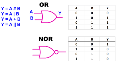 Likewise the OR gate is simple, straightforward, and can be drawn as an alternate symbol. With the OR gate, the output with be high if one OR the other is high (including if both are high). The NOR has the same behavior, however, it inverts the output. Compare the truth tables for both the OR and the NOR gates shown here.
XOR
I also recommend learning to think about logic as not just highs and low, or ones and zeros’ but also about the logic of true and not true. Particularly in higher integration situations we save the actual polarity of a true signal until the last moment when it actually gets assigned a pin and polarity as it leaves the chip.
Another logic function is the “exclusive or” function written as XOR. It has the function that the output is true if, and only if, one input is true. An example of a cool use of this is as a programmable signal inventor that can be made as shown above.
High Impedance or “Hi-Z”
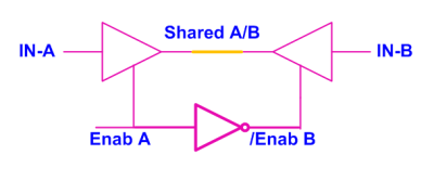 In addition to highs and lows we also have a third state of high impedance or “Hi-Z” state. This is the state that a tri-state enabled device (referring to the three states: high, low and hi-z) when the output is disabled. This is how multiple devices can access a common resource such as memory, basically jumping on and off the common bus.
Open Collector
Another way to combine outputs is to use open collector outputs which drive the line in the low direction only, they are either off or low. Multiple outputs may be combined without fear of them shorting to each other as they can only drive low while no one drives high (high is passive). As a result we end up with an AND logic function where the output is high only if all outputs are in a Hi-z state.
Not just digital devices use open collector outputs, shown on the right is a very common quad analog comparator that uses an open collector output which makes it a good match for converting an analog signal to a digital. We can combine two pieces of analog information due to the ability to connect two open collector outputs. Here in this window comparator a signal has to been “approved” by both comparators, when both are true the resistor is free to pull the output high.
Logic Chips
Finally there are standard logic chips that may be used as general purpose functions such as the 74×139, two to four decoder with enable. Looking at its logic table we can find an unusual function by selecting which of the outputs we choose.
Before I end I wanted to put it together and show some simple logic combined with the equation nomenclature. This nomenclature can extend to huge projects or high level languages while staying pretty straightforward. Above is a simple circuit that demonstrates using parenthesis to indicate order of operation.
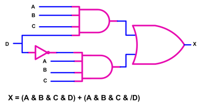 To the right is another circuit, can you spot the risk of a glitch?
In the next installment I will talk about the electrical properties of common logic families and also introduce Programmable Logic Devices and the software that allows us to describe hardware using a text editor.


nice post, in the last circuit the input d is not relevant for x which always be depedant to a, b and c. (with some boolean algebra:x=abc)
Have another think about “can you spot the risk of a glitch?” Hint: It wouldn’t happen in your simpler version.
My guess (and I didn’t read the rest of the comments):
There will be an output of 1 only if A,B,C is 1. If any of A,B or C is 0, the AND gates at the left won’t activate no matter what D does.
So, if we put A,B,C at 1, in theory no matter what D does (1 or 0), one of the two AND Gates should activate (thanks to the NOT gate), sending a 1 to the OR gate and to the output.
My thinking is that the risk of glitch is when the NOT gate has a switching delay or a “response time” to their input. The Texas Instruments 7404 Datasheet (NOT gate chip) states that there’s a switching delay of 9-15ns. At high enough frequencies, it’s possible to induce a “glitch” where D switches too fast for the NOT gate to keep up, potentially varying the output between 1 and 0 even if A,B,C is 1.
Hope that’s clear, and please correct me if I am wrong.
Thanks!
The glitch is also there at low frequencies. The length of the glitch is the propagation delay of the inverter. At low frequencies, the glitch might not be a problem, but it’s there just as well. The length of the glitch doesn’t change with frequency, so the higher the frequency that this circuit is required to switch at, the more significant the glitch becomes. But it’s always there.
Please pick a annotation style and stick with it. You seem to change the style from example to example. At 9:30 in, you are showing an example with ‘&’ representing a logical AND and ‘/’ representing a bitwise inversion. Then the very next example 20 seconds later you are showing ‘*’ representing a logical AND and a ‘!’ representing a bit-wise inversion. I would not have even shown more than one annotation style outside of the overview.
It is relevant for introducing glitches through.
Something tells me he’ll do simplification using boolean math at a later point. Had he simplified it, he may not have been able to make his point.
Thanks for producing this video. I’m familiar with these concepts but was not aware of alternative notation. That’s very useful information and I’m very surprised it wasn’t presented to me when I took basic digital theory.
Yes, had I left C off there would still be a switching hazard when D switched, and this is usually where someone gets into trouble is not recognizing the common part. I wanted to be real clear and not confuse someone with the A&B and the A&B&C
Does anyone think its work getting old Altera DIP PLDS? Im getting a few dozen extremely cheap but i have no idea if its still possible to buy/make a programmer for them?
I will be doing a whole segment on PLDs and then CPLDs. I only got partial success trying to find software, devices and programmers for PLDs that all play nice together.
BTW, I was looking at 5V DIP as the first line for hobbyist and then see how far down the rabbit hole we have to go (3v SMT) to get a good usable PLD platform for playing day to day use.
Well someone from Poland has a huge surplus of Altera EP610PC-35 all DIP 24. I was temped to buy it off him but them i remembered how hard it can be to program these old devices! What do you think? worth a dig? If it is possible to program these 300 gate devices they will make for an interesting breadboard experiment!
Send some to me.. ;) I’ll take good care of them :D
Unless you happen to have the old data I/O lying around. You’ll still need the fitter program that spills out the bit streams.
The old XC9500 5V parts if you can still find them are the ones you should stock up for. I wish I stocked up more of those.
Dang! Would love a 5v tolerant CPLD! Are there no more 5v tolerant CPLDS in the market?
Yes, In the video is a very brief shot of a 5V CPLD pinned out to .1″ headers that could fit a solderless breadboard or other such as perfboard. I will be going through it and am currently researching an opensource in circuit programmer for it in addition to the cheap clones.
The XC9500XL 3.3V are still on the market. They are probably one of the few 5V tolerant CPLD. Also designed for real life – handles the overshoot/undershoot if you keep it under the absolute max specs. Use a series resistor and that would help for that.
from the Absolute maximum rating:
> During transitions, the device pins may undershoot to –2.0 V or overshoot to +7.0V, provided this over- or undershoot lasts less than 10 ns and with the forcing current being limited to 200 mA. External I/O voltage may not exceed VCCINT by 4.0V.
This! all of this should be required for CS degrees.
At least in my university this is on a obligatory course.
Mine too. Was one of my favorite classes too.
Mine two…we didn’t use hardware though just simulation software…went from gates to full adders…
nand 2 tetris is great but can’t do much with it after…all the time you spend making the different chips…if it was done like on say, a DE1….you could always reuse all your VHDL for other stuff instead of starting from scratch…
the glitch on last circuit is the delay imposed by the inverter. it will cause X to have a spike the width of the delay of the inverter
I think so too. I forget how this is remedied. Maybe next time.
You supply a covering term that is true even during the transition. :) There is a trick to catching the really complicated instances, the trick for me will be to remember the technique well enough to talk about it 100% accurately. Hmmmm…. is there an emoticon for “old and burnt out”?
In practice, you rarely use complicated discrete logic, and if you use an FPGA/CPLD, then you would usually register the outputs, so glitches aren’t a problem.
Bzzt – not always a safe statement.
Be aware of “CDC” (Clock Domain Crossing) issues: you may have a safely synchronised control signal (e.g. double-registered grey-code) that is selecting ‘safe’ stable data (static for the entire time of grey-code+sync-delay). If that mux select structure is not ‘safe’ (i.e. can produce glitches like Bill’s example) then if one of the un-selected data registers changes value then it can result in meta-stability issues appearing on your ‘safe’ data.
An example of this is in asynchronous FIFOs where you use 6 data banks that are cycled around and the destination clock domain receives a grey-coded value of what the send clock domain has written to. Along with the destination domain sending back a similarly grey-coded value of where it has read to, you avoid reading and writing data banks that are ‘active’ (needing to be stable in the destination or unstable as they’re being updated in the send domain). However, while a simple OR-of-ANDs structure is often assumed, how that is constructed by synthesis tools can vary and unsafe structures created resulting in glitches.
Well, yeah, a lot of things are no longer safe when dealing with clock domain crossings.
Hi Bil. Great post. BTW, which software did you use to make the circuit diagrams? Looks good.
Sadley I used Visio as I have to make something that will print, overlay in video or make embedded images and not be fighting what a CAD system wants to do.
Those notations are horrible and sometimes even wrong. And why not just use the Boolean algebra notations?
different applications use different notations. For instance, you will find != in C along with & and ^ or even something like ~ used. All with respect to bitwise operations. This is important because after paper boolean math comes the Application of that math. I was happy to see other ways of writing the notation, I anticipate running across them when I enter the industry after school and imagine it’ll be expected I know how to read them. I would suggest that instead of dismissing things your not familiar with as “wrong” you investigate why you see them as wrong. You’ll find that more often than not they are just different. At least that’s how I approach this sort of thing.
To make it short: I am missing the necessary definitions and formalism. And it doesn’t matter if it is applied math or not.
Not gate: Y = A is obviously wrong without further definition, because the ‘=’ sign is already defined as ‘equal’.
AND and XOR gate: Y = A & B. Without further definition wrong, because it implies that AND and XOR gate are equal, which is a contradiction.
It’s unfortunate that there are many symbols for logic but that’s the way it is. There are many correct notations for boolean logic and you will likely need to learn most of them.
Not just learn the different nomenclatures but also recognize which family of nomenclature that is in play and dare I say, start thinking in that nomenclature like shifting gears on a bike. Looking for an error in logic is much easier if your “eyes” are doing the decoding. :) Thanks for the feedback M. Bindhammer, Travis and Darren.
Function of the Not gate Y = A? Should be Y = ¬A :)
So happy to see this comment. I thought I was the only one who was puzzled by that.
Might be simplest just to use AND, OR, NOT as words. We’re not short of bandwidth for the extra letters. Since it’s supposed to be educational, and it’s starting at the bottom, people who might benefit from this aren’t going to have the habit of automatically recognising the symbols. Same way, when you learn Japanese they start out using the Latin alphabet. At least it does on my Nintendo DS.
Bil are you gonna tell us what the glitch is? I’m too lazy to get pen and paper out. I’ll understand it AFTER you give the answer!
for a future topic, I’d like to have a better understanding of when to pick the various logic families (74LS, A, H, HC and so on).
That’s a great idea, actually. The trick, I think, will be designing something that works with one family and fails with another.
The purchasing department is usually in charge of finding the family that fails. >:)
+1
There was a fair amount of art to knowing which were best or viable alternatives for the various families and that was just at 5 volt. In some ways the different voltages have made it easier as there are fewer choices than once were depending on what supply voltage you have.
the basics of ttl and cmos and 3.3/5/1.8 (etc) are one thing; but I’d like to know what the real decision process is on how to correctly pick the ALS vs LS vs HC (etc) families. what is the down-side to just picking the fastest or lower power chips? I bet there is a lot of trade-off in picking one vs the other (why would vendors spend so much time/money making and stocking all those variations if it wasn’t justified?). insight from the field on the decision process of picking a chip type would be very welcome. also lists of what would be redundant or not worth going for, anymore (probably the base series, 7400? does anyone use 74S series or only LS? why use H when you can use A and so on.
the voltage stuff is not hard to understand; but if I’m trying to pick gates for high speed, is there an obvious choice or is it still a trade-off and by picking the fastest gate, maybe its more finicky or less stable or needs more layout finesse?
I love the question! I just didn’t think that there was any interest in such a discussion these days. tekkieneet is right on about the fact that there was growth from into or out of a family and that drive strength; symmetry can be really important sometimes and early stuff wasn’t so symmetrical, speed; too fast creates issues but fixes others, and power dissipation; sometimes less current meant less oomph when oomph was needed.
Typically we wouldn’t use an S part if an AS or ALS was available. LS was more like fast TTL insofar as speed and was the true jelly bean of our era. (It became very hard to get LS parts for a year or so around 1981 as all of the handheld game machines dried the market up). For example S parts used lots of power to get just a few more nanoseconds of speed while creating a fair amount of noise in the process. Meanwhile LS has paltry output high drive unless talking strictly to other LS devices. Families like H for high speed kind of came and went as other parts met the speed requirements while bringing other aspects like lower power dissipation.
The F fast parts seemed to come from nowhere and just plain saved the day sometimes, other times someone would use an F part and if they didn’t take the care you would with a fully charged fire hose, the result would be everything getting all wet. (It drives hard and fast). With that said the F parts did well as far as passing FCC if treated correctly or at least in my experience.
Driving a bus vs just some random logic also helps the decision process, symmetry becomes important, the ability to drive a load equally fast in opposite directions, particularly with some capacitance on it, as does output impedance. Balanced is better here also.
CMOS parts became HC versions of TTL which could drive hard (and land soft) surprisingly, and low power consumption, but hated TTL inputs, hence the HCT meaning TTL compatible. There then became an AHCT version then where the goal, as with most “A”s was to keep a feature like power but make it act more like the other parts in speed. Anything CMOS other than sourcing a lot of current in the high direction was due to power dissipation for the most part. These days I believe that there is a lot of CMOS behind the most common parts.
Lots of families with “A” in their name now which would be where I would start to look for parts just out of habit.
Most of the time we start by selecting a family for an attribute: power dissipation, speed or even cost. We then look at what the ramifications are of fanout/drive, availability and in my case designing consumer products where I would take into account how noisy the part could be as far as meeting FCC requirements when measured by an antenna, or as far as creating noise internally that became hard to live with Designs would then be checked to see if termination and other design techniques increased speed, decreased noise, reduced power, etc. Inevitably the Purchasing Dept. gets back to you and asks what other part families would also work or production would look at one spec and ignore another and do their own swapping of families.
that info is gold! thanks!
I bet there could be an hour long video just from this topic, alone. might be interesting to look at some designs and comment on them; “this is good, he picked X because of Y and I agree” or “wow, did he really use X this circuit really should have used Y” and “well, its ok he used X, but could have saved money because Y is a lot more common and easy to source in a pinch”.
going thru good and not so good designs would be a great educational video. and as you touched on, if you don’t even KNOW what you are going to encounter south or north of you (maybe you are just a module in a DIY system and you have little control what’s going in or out of your subsystem) – what’s a good safe way to approach it.
slightly related (only slightly): I’d also love to see info about how to protect user interface inputs from static. more and more ‘makers’ are adding buttons and knobs and displays and controllers are sensing them. quite a few times on my own builds, I have been able to static zap my front panels during some seasons (where static builds up) and commercial gear seems a bit more resistant than most DIYs to this; so, what are they doing and can we do the same things so our builds are as robust in a harsh-ish user environment. I mention this because some logic families may be more twitchy to emi/rfi and maybe even static hitting a chassis (that is even grounded) may cause some gate types to freak out more than others. if we are trying to design for stability (conservative) what are some tricks or things to avoid?
Use series resistors e.g. 10K from panel, on the PCB side use silicon signal diodes (not rectifier diodes) clamping diodes to power/ground. This would help to limit the amount of ESD to the chips. If noise is an issues, small value caps (1nF to 10nF) across input on the chips facing the panel is a good way to block spikes and in some cases ESD. As usual, good power/ground plane and decoupling caps with low inductance. etc.
There are some families with more rugged inputs by looking at the absolute rating input range, latchup currents, ESD ratings etc.
Also TVS for protection.
I used to design for IEC 801-2, the infamous static finger test. It was with love and adoration we adopted the TVS “transzorb” type of fast avalanche parts which can deal with fast rise times.
Some of the family were historical as they didn’t have all the families out at once. So it makes little sense to use a 74S or 74H or 74L parts when there are newer versions.
Sometime you pick a family because of drive strength (higher current, symmetrical, series termination), sometime speed, sometimes power consumption, sometime with better I/O: more rugged/ 5V tolerant / hot insertion / bus hold etc.
that’s the info I was looking for. ‘no reason to pick X Y or Z if you have A B or C buyable and at good stock numbers’. stuff like that.
you see all of what mouser/etc offers – but what should we prefer and what should we ignore?
some general rules to start it off would be nice (which you already did, in fact) ;)
LOVE this sub-thread, thanks everyone for your insight! I’m currently neck deep in Chapter 9 of ‘The Art of Electronics’ (the previous edition) which really gets into the weeds on EXACTLY this topic. I ventured down this rabbit hole while poking around some ECL circuits in some old Tektronix gear.
Assuming that you are not handicapped by only using DIP packages, the LVC/LCX seems to be a complete family with logic parts. There are other specialized families with only bus drivers etc.
Voltage: 1.65V – 3.6V (for some reasons the single gate packages extended that to 5.5V) The usual goodness of low power, relative fast part, modern packages and relative cheap.
Input (Absolute Max): -0.5V to 6.5V i.e. you probably want to stick with 0V – 5.5V
Unlike the old CMOS with the ESD diodes tied to VCC, you don’t have to worry about voltages at input when the part is unpowered. Good for hot swap etc The way to spot this is in the absolute max part of the datasheet. If it say input voltage Vcc+0.5V, then there is a ESD diode.
At 3.3V, you can use them to drive or receive TTL signals. Symmetrical sink/source current 24mA (at 3V).
Things to watch out for though is for parts with fast rise/fall time, you have start looking at series terminations, low inductance break for decoupling – the usual signal integrity stuff. General advice use the slowest part to get the job done.
^breakout. Just have a decoupling cap somewhere is not enough. There should be a low inductance connection to the power and ground rail i.e. a plane. etc
A very low ESR decoupling cap can actually cause a secondary issue in in that the inductance if the trace will resonate with the capacitance of the decoupling cap. I usually “detune” the supply circuit by removing stubs I.E. providing 2 or 3 directions for current to source from. The “last mile” of the DIP package lead can still impart it’s own inductive opinion however, SMT goes a long way towards getting rid of the “sky aerials” that where the DIP leads.
I have been using SMT parts at least more than 15 years. I don’t do DIP. These days my preference are QFN parts. No pins to bend and good SI.
The usual bulk power supply rated tantalum caps would help with the damping.
I consider the tant at the frontend to be a macro filter, Probably more for supply and wiring characteristics, and to add a lower freq pole .
For trace inductance/decouple cap interaction I think of the last inch down to half inch; what can start as a ground lift on a pin becomes a bell ring worst case or a sudden current starvation on the first half cycle of what the resonant frequency turns out to be.
Tant cap can provide some RC damping too – hundreds of mohms worth of ESR is AC coupled across the rail.
Modern packages have much better layout with shorter lead frame to the internal power/ground connection as well as multiple power/ground pair if they have wide bus. They are already design with SI in mind. For SMT packages with decoupling caps within 0.1″, to 0.2″ from the supply pins should be able to help to filter the disturbance before it gets into the power rail.
I will be demonstrating software that uses the various notations before the end of the series. Depending on what an engineer is doing they may be exposed to 3 different nomenclatures in a few hours, my feeling is that it is good to be able to interpret multiple styles on the fly.
The “+” on the hand drawn OC schematic could be clearer as a different symbol, this was unfortunately an old habit.
Bil is the best part of HaD!
Not to be too pedantic, but Karnaugh Maps are pronounced “Car-No”, not “Car-Noff”. (http://en.wikipedia.org/wiki/Talk%3AKarnaugh_map#Pronunciation is one reference example). Just want to make sure we don’t get a new generation of hackers learning it incorrectly. :)
And yet it sounds like I am putting “ffs” on the end when I say it. :) I blame growing up in the midwest and hitting my head on the see-ment when I was young.
ouch. do you need a glass of wudder?
lol
And here I thought you somehow stay too long in the south and picked up the drawl. :D
Good introduction! It would be nice to include a discussion about pull up/pull down resistors, since this topic is sometimes confusing for novices.
Ya, you also here me allude to capacitance without having time to say whats that all about. I used to say there is no such thing as a pull-down resistor, it might be less true in these days of CMOS-like input currents, though I would still think it to be bad form.
I will include something about this when I talk about the electrical properties, thanks!
You haven’t used ECL/PECL!?
There are 4-5 of books on my workbench generally and can be seen sitting either on top of or next to the HP function generator on the shelf to the left. Two are on ECL/MECL/PECL designs and guidelines. :)
That was the good old days around the dot com era. I was suddenly face with 600+bps and later on 3Gbps world from a 30-60MHz background. I have learnt most of the high speed differential signaling/clock trees from electronic copy of those books when I switched job. That and reading up a lot on datasheet/app notes/SI mailing list/scope measuring techniques help me quite a bit on my career as most other engineers don’t or have time to do that..
The second text line in the inverter image (after the video) is wrong, the line over the A is missing.
Lol… yes it is. It was there when I shot the video portion.
i was thrown off by this series expecting some very basic stuff but now i have high hopes … just the first video i learned something!
Holy crap Bil, you are one hot man.
Great post!
I would have started with diode-diode-resistor logic to explain AND and OR, and then use transistors for inverters (and open-collector). Then go to totem-pole (high-Z will probably be explainable with a single statement at this point), then explain logic equivalence and differences between US, EU and IEC logic symbols. Glitches can be introduced at the same time as an XOR port: just draw its equivalent in AND/OR/NAND gates, tie the inputs together and explain that it takes just a little bit shorter or longer for a change go one way vs the other way.
But this works too :-)
Bil, this is great stuff man! I really enjoyed this! Great bit of work here mate and amazing effort!