Most hobbyists say that it is easier to build a functional prototype of an electronic device, than to make the enclosure for it. You could say that there are a lot of ready-made enclosures on the market, but they are never exactly what you need. You could also use a 3D printer to build a custom enclosure, but high-end 3D printers are too expensive, and the cheaper ones produce housings which are often not robust enough, and also require a lot of additional treatment.
Another way is to build the enclosure out of FR4, a material which is commonly used in PCB production. Such enclosures are low-cost, with thin walls but yet very strong, nice looking, pleasant to the touch and have excellent thermal and moisture stability. FR4 offers some more possibilities – efficient wiring with no wires inside the housing, integrated UHF or SHF antennas or RFID coils, capacitive switches, electrical shielding, selective semi-transparency, water or air tightness, and even integration of complex mechanical assemblies.
Here I shall explain the process of building those “magic” enclosures. It is based on nearly fifty years of personal experience and more than a hundred enclosures, built for most of my projects. Here are two examples – this case for a hardware password manager is just a few centimeters long, while the other one (protective transportation cover for my son’s synthesizer) measures 125cm (about 49 inches), and yet both of them are strong enough to withstand a grown man standing on top of them.


The global approach is simple – you take the sheet of single-sided copper clad FR4, cut it and solder the parts together. That sounds simple, but there are a lot of details which should be met if you want to get top results. Please read about them carefully. You might be tempted to skip some of the steps described here, but if you do so, you will most likely end up being disappointed with the results.
Tools and Materials
- A lot of single-sided FR4, preferably 1.5 mm thick (it is classified as 1.6 mm, but when you measure it, it always turns out to be 1.5). In some cases, you will need some other thickness.
- Medium power soldering iron (about 40 W, or 60W if it is temperature controlled).
- Soldering wire with rosin core, about 1 mm diameter
- Soldering flux
- Transparent self-adhesive laminate
- Safety blade cutter with a lot of spare blades
- Fret saw frame
- Ruler
- Drill
- Fine rasp
- Fine sandpaper
- Ferric chloride solution
- Undiluted alcohol
Design Concepts
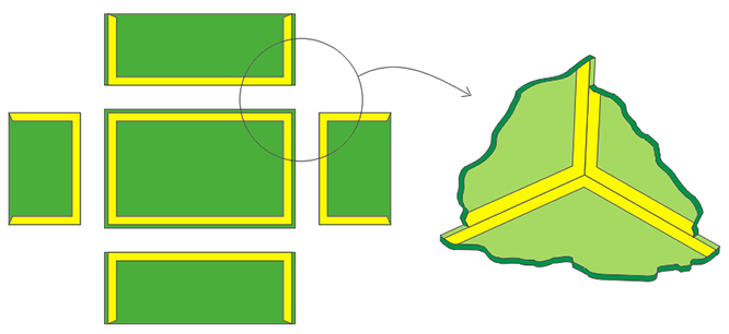
There are several general design concepts for enclosures made of FR4. The first uses the main PCB, with all electronic components, as a mechanical base on which four walls will be soldered. Typically all electronic components should be soldered first, then PCB is tested and finally the walls soldered together.
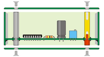 Main PCB must have a copper area around 4 mm wide along all of it’s edges and large pads for spacers. Top and bottom covers are very simple and they need no copper areas, so you can also use acrylic, aluminum, plastic, etc. This concept is suitable for simple projects, which contain only one PCB. It is not advisable for thick enclosures, as it would be inconvenient for maintenance.
There is another approach which is suitable for bigger and more complex devices, as there is a lot of free space which can be organized according to the requirements of the project.
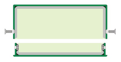 You should leave copper areas for screw nut soldering, but do not solder them before the whole enclosure is finished. After the job is done, you can close it and bore the holes at the inside walls, so they will fit perfectly with the outer holes. Then you can solder screw nuts, using a lot of flux.
Note that not all screw nuts are easy for soldering, so you will need some experimenting. In my experience, nickel plated brass screw nuts are the best in this regard, but sometimes they can be hard to get. So I use M3x5 mm spacers (but not those made of aluminum), which are very easy to solder.
If you want to make an enclosure without screws, you can use friction to hold two subassemblies firmly together. Finish the upper (outer) part of the enclosure first, and then adjust positions of inside walls on the lower cover. Outer walls will always be slightly inclined to the center (the reason for this will be explained later) and it will create some friction when you close the box.


To adjust the tension, solder the inner walls to the lower plate, but only at the central point, trying to maintain the right angle between the walls and the bottom plate. Then try to put on the top cover. It might be too loose or too tight, so you have to tune up the right position for a tight fit. Repeat this for shorter walls and then solder the length of the walls to the lower plate, and to each other. You should also rasp the connecting edges of the inner walls, to make space for solder which keeps the outer walls together.
The tightest joint between inner and outer walls should be at the center of the walls, with the possibility of a gap close to the edges, so the inner walls need to be slightly curved, like show in the center image above.
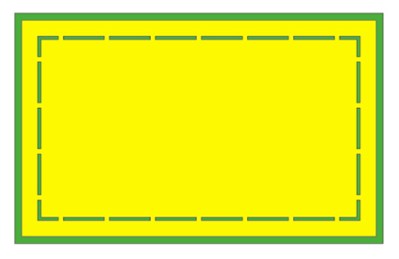
Generally, all plates should be made of single sided FR4, but in some special cases you’ll need double sided. Try to find the double sided wall on the drawing show to the right in the gallery above.
Those were general concepts, but all combinations are also possible. Soon we shall see that some applications are so complex that it is hard to classify them.
To etch or not to etch
 Although it is possible to build the usable housing without copper etching, it is highly recommended to etch all plates, and to leave only areas (about 4 mm wide) which will be soldered. This will bring a lot of advantages. First, it is much easier to solder the narrow copper areas, when the surrounding copper does not consume a lot of heat, so the risk of overheating and damaging FR4 base is much lower. Second, you will get a neater interior. Also, if there is no bare copper, no corrosion will take place. The danger of short circuiting is lower, and so on.
If there is a demand for a shielded case, for HF applications or a light shielded area, this pattern is recommended. The only disadvantage of etching is that you must plan all details while designing the enclosure, as there is no undo after etching. If you omit some area that should be used for soldering, you can not add the copper layer later.
Designing
Take some time to design the enclosure carefully, as every miscalculation in this step may ruin your effort. Take good care of which piece will overlap with another one, as it will affect the position of copper traces. The thickness of FR4 used must be taken into calculation for the dimensions of overlapping plates.
Use some CAD program, or draw the whole enclosure with colored pens. It will serve as a useful reference while cutting and assembling the parts. It is good practice to build at least a few millimeters larger enclosure than you planned at first. In most cases, it will pay off later – no matter how carefully you measure and plan, sooner or later you will need some extra space.
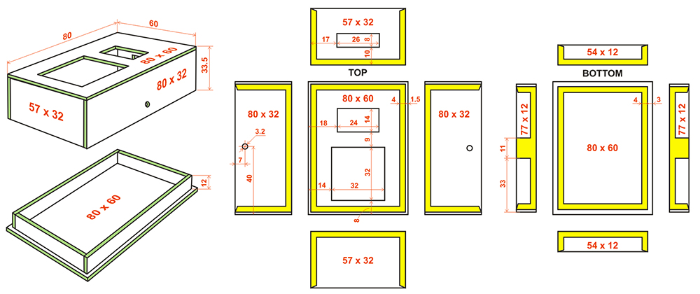
There are a total of 10 sheets here. Draw each of them in detail, including etched copper positions and all dimensions, or at least those which are not considered.
Cutting
If you are fortunate enough to have a CNC cutter, then use it to cut FR4 parts. Any mechanical or water jet cutter will be fine, but do not use a laser cutter, as the reflection from the copper surface can damage it. Otherwise, you can use some hand tools, like a fret saw frame. A safety blade cutter can also be used for cutting straight lines, but the demand for significant force and accuracy can be frustrating if you are not experienced enough.
Try it, just press a metal ruler firmly with one hand, take the safety blade cutter in the other and make a V-cut. You should make about 5-10 blade passes on each side of the FR4, starting lightly until you make the good scratch, and then increase the pressure until you use as much strength as you can. Make the V-cut on the copper side first, as FR4 is transparent enough to let you see the line on the other side, so you can align both V-cuts precisely.
If the blade is sharp enough and you use significant force, grooves on both sides will be deep enough and if they are well aligned, it will be easy to break the sheet by hand. The cut line will be rough, so you should treat it with the fine rasp.


Of course, you can’t cut curved and inner lines with a safety blade cutter, so in that case you have to use the fret saw frame.
Check the dimensions carefully after each step, and do your best to get as accurate dimensions as possible (try to limit the error to less than half a millimeter). After cutting and treating, wash the copper side with some powder detergent, abrasive enough to clean the surface but not to damage it.
Note: FR4 is made of fiberglass matting which has been impregnated with epoxy resin. Small particles of glass, which are released during treatment, may cause temporary skin irritation to those who have sensitive skin. In that case, use protective gloves and wash your hands up to the elbows after work.
Laminating and copper etching
The goal of this step is to create the mask for copper etching. You can also apply the photoresist process, but it is much cheaper and easier to use any kind of self-adhesive laminate, preferably transparent.
When FR4 pieces are dry and clean, stick the laminate sheets on the copper side, avoiding bubbles and dirt. Use a super-thin permanent marker to draw all lines precisely on the laminate, according to the drawing mentioned above in Design Concepts and use the safety blade cutter or art knife to cut the laminate. Peel off all areas which should be unprotected during etching.
Use Ferric Chloride solution to etch the copper layer. This process is well known to all hobbyists who make their own printed circuit boards. After etching, remove the laminate and wash all pieces with powder detergent.
Assembling
Hold your breath, this is a crucial step. All copper surfaces should be tinned before final soldering; use a lot of flux, as a lot of flux means a good joint, and the good joint is what we need here. Don’t attempt final soldering without tinning, as it could result in a poor joint, damage the FR4 base, and reduce your ability to maintain the exact positions in assembly process.
It is hard to ensure alignment on all axes (X, Y and two angles) while soldering FR4 plates together but, if you follow the procedure, you can tune one parameter at a time.


First, take care of X position (black arrow) only and ignore the accuracy for all others. Solder two plates at one point, close to one of the edges.
Next, you can tune the YB position at the other end of the soldering line. FR4 is elastic enough to compensate for the initial misalignment, but X position, which was already adjusted, will remain intact.
Now it’s time to readjust the YA position at the first point, without worrying about first two tuned positions (X and YB), as there is no way to spoil them any more. This should lead to the perfect alignment of the whole soldering line.
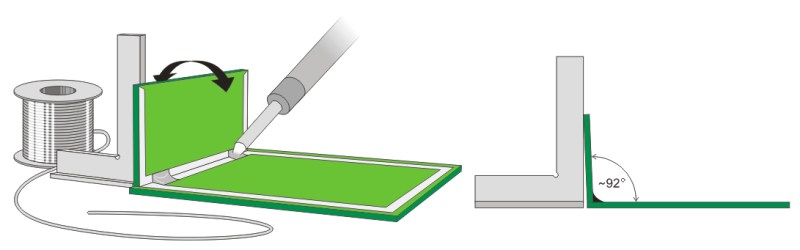
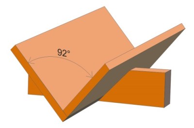
The only thing left is the angle between two plates. Use a square or triangular ruler for reference, but do not adjust the exact right angle between plates, but rather make it slightly obtuse. You can fine-tune the angles at each edge separately, especially if the plate is long enough to enable bending between them.
When all positions are adjusted and checked, you can put more soldered points between plates, checking the angle for each of them. For shorter plates it should be somewhere in the middle, or at every 4-5 cm (1.5-2 inches) if the soldering line is longer. Then you solder the whole line, but try not to melt the already soldered points, as you could spoil the plate angle and position. When you have finished, you can return and solder the missed points.
While the solder is cooling, it shrinks and pulls the upper plate for about two degrees, so the final angle will be close to 90 degrees. If it is obtuse still, make one more pass with the soldering iron (with no force applied), and look how it shrinks. If it is acute, then make one more pass, applying some force with your hand.
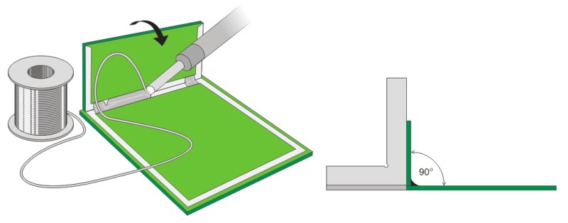
Apply the same process for all walls. After that, you can solder the walls mutually. At this step, you can’t start from an obtuse angle, so you will get slightly acute angles at the end. You can ignore this, or even use it to obtain a tight joint, mentioned above.
Take care not to be too slow while soldering, as you could overheat the FR4, and especially not to press the soldering iron too hard. This will deform the FR4 base, or even unstick the copper. FR4 is transparent, so if you see the white areas from the other side instead of dark brownish copper, you can be sure that the copper is detached from the base. It may be useful to do some experimenting with FR4 leftover parts. If you want to see for yourself how much mistreatment the material can endure, you can try to break the bonds with your hands after proper soldering, or even test the bonds where you used too little or too much solder, or where you held the soldering iron too long or pressed it too hard.
 It might also be helpful to make a special wooden tool for assembling. You probably get the idea from this drawing. Soldered joints will be even stronger if plates are held about 45° in relation to the horizontal plane, so that the molten tin connects to both panels equally.
When the assembly is complete, use the rasp to process all edges, then polish them with fine sandpaper. Wash the inner side with alcohol, to remove all remaining rosin core and flux, if you used it. At the last step, wash the whole enclosure with detergent and a lot of water, dry it and enjoy the fruits of your labor. If you followed all steps carefully, you will have a good reason to feel proud.
 Cutting, laminating and etching are the hardest parts of the process, so why not just order all the sheets from your PCB supplier? Of course you can do it, if you don’t mind the price. In some cases (for prototyping and very small scale production), the final price of the unit could justify the cost of PCBs. It sounds like a dream come true – avoid the worst part of the job, and get all the parts with perfect accuracy, heavy duty paint and overlay letters and signs. This is one of such project.
Printed conductors
 You can also make the printed conductors inside the enclosure walls, so you will have even complex wiring with no wires. This, of course, requires careful planning during the design process. Here is part of an enclosure in which copper layers are used both for mechanical subassembly and electrical interconnection.
It is also easy to implement capacitive switches, inductive couplers, reed switches, Hall Effect sensors and RFID, UHF or SHF antennas in enclosure walls. Printed wiring for LED indicators can contain SMD current limiting resistors and soldering pads which are close to LEDs.
Transparency
Copper is not transparent, but FR4 has diffuse transparency at the etched areas. Some thin (0.8 or 1 mm) FR4 boards add a nice milky or yellowish tint which can look good when used for indicator LEDs, or even night lamps or some LED Art gadgets. The following examples combine transparent front boards with conductors which are implemented not only in FR4 copper traces, but also in the kite’s tail (which is AC cord) and black sticks (M3 spacers dressed in heat shrink tubes). Black borders are copper traces left for soldering.


Unfortunately, most manufacturers put the coloured logo marks on FR4 epoxy base. There is no way to erase the ink, so this material is hardly usable for such applications. To make things worse, there is no way to see those marks before you etch the board. Yet some FR4 boards do not have those marks and, with a certain amount of luck, you can find and purchase them.
Bending
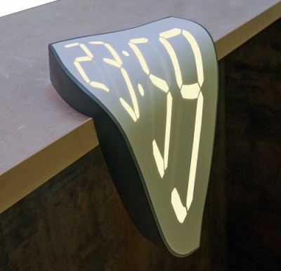 FR4 boards can be bent to a certain extent, so it can be used for softly curved walls. Here is a digital clock bent like a pancake, an homage to Salvador Dali’s famous picture The Persistence Of Memory.
The front board is made of .8 mm FR4, which is quite easy to bend. The 7-segment areas were designed in a CAD program, used to cut self-adhesive laminate for etching process. All other boards are 1.5 mm thick.
When you solder such curved walls together, be very careful not to overheat the boards, especially if they are 1 mm thick or less. Mechanical tension of the bent FR4 plate makes it extremely vulnerable to overheating, and even the slightest deformation is impossible to repair. You need to fix the plates in their final position and shape, and briskly solder them together.
Mechanical assemblies
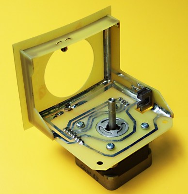
It is even possible to build the mechanical units, possibly combined with some prefabricated metal or plastic parts. This is particularly valid for projects which contain both electronic and mechanical components, as it enables efficient placing of drivers and connectors close to motors and solenoids, sensors for home detection of moving parts, wiring using printed conductors, easy placing of indicator LEDs for debugging, integration of electronic circuits on the enclosure walls and so on.


Here are some examples of such assemblies, which explore many possibilities of FR4 enclosures.
Conclusion
Proper use of FR4 can greatly improve projects and make them look like high end products, even if they are built in amateur conditions. It should not be neglected as a building material for hobby projects or for small scale production.
Of course, craftmanship is of vital importance, so you will need some experience under your belt to get top results. Don’t give up, and soon you’ll be proud of the appearance of your projects!
 Voja Antonic works as a freelance microcontroller engineer in Belgrade. His first microprocessor projects, based on Z80, date back to 1977, just a few years after the appearance of the first Intel’s 4004. He assembled the firmware manually, by pen and paper. In 1983, he published his original DIY microcomputer project called Galaksija, which was built by around 8000 enthusiasts in the former Yugoslavia. To date he has published more than 50 projects, mostly based on microcontrollers, and released all of them in the public domain.


Awesome article! Brings back memories to years ago, when I soldered such as enclosures.
Yup, this has been a common technique for hams and RF engineers going back at least as far as the 1970s.
Yep, been there, done that, but it’s still nice to see a primer on the subject posted here. :)
Sometimes new dogs need to be reminded of old tricks.
How do you ensure the edges are not sharp or fibrous though?
Sorry Mystick – Replies are too deep forgive me for piggy-backing on your original comment.
@Waterjet – “if the string is too tight it will snap, it the string is too loose it won’t play.” comes to mind.
I imagine the grit or grade of the grinding material would be the prime factor. A rasp file would leave it too fibrous, where as a fine file would make too much glass dust and take a long time.
I’m sure a small 9V DC motor with a sandpaper cylinder would limit the exposure and make quick work of the task.
I think however the issue that may have been overlooked is the GLASS DUST. As you are well aware WATERJET. and we DO need to point out. Fiberglass isn’t asbestos but it is Microscopic GLASS SHARDS and can really mess up ones lungs.
Well it has to be said since not everyone has read Diamond Age and current non-fiction studies do indicate carbon fiber/nano tube particles aren’t healthy to breathe in. Heck man, Miners suffer from black lung but the weird one was teachers suffer from White Lung from the chalk. Now you have an excuse to sue your old school district for having the teacher make one ‘go clean the erasers”.
Whoa! THis one goes in the bookmarks file.
THANKS so much for writing this up for us.
I’ll second this and add that it sets a good example for style/format example for tutorials on HAD.
This is fascinating… I’ve never run across this idea before. Thank you, [Voja]!
This is an incredibly useful article. As an alternative to the jig described in the article, does anyone have suggestions for some sort of corner clamp that could be used to hold the boards at the proper angle for soldering?
most cabinetry clamps will be at exactly 90*, so your best bet is homebrewing. however, the jig shown in the article is very basic. I’m sure an enterprising maker-fabricator could come up with something more elegant
You could start with the 90* cabinet clamps and shim near the top to widen it out a bit.
Excellent description of a classic technique :)
Awesome ! that’s what I’d like from Hackaday.
Excellent
RF engineers and hams have been making cases like this since the 1970s, possibly longer than that.
Yeah, and? Still a great and beautiful article….
That’s exactly what I’ve told in the article, I used it almost 50 years ago
Beautiful work. This opens up many possibilities, i.e. filigree work on the outside using double sided boards.
Have you tried filleting the joints with a strand of copper wire to add strength?
Yes, the thick copper wire is required if the angle between boards is very obtuse, but it is of no use for the right angle, as the bootleneck is not in the soldered joint but between copper and FR4. That’s where it breaks.
bootleneck
He meant “weak point”. But since I can’t write a word in Serbo-Croat, I can hardly criticise him for getting it wrong.
I agree with Greenaum – and I kind of like it. Just like we have a bin of “Eanana Plags” at work and nobody has relabeled it because it’s too awesome.
“Eanana Plags” really had me stumped for a minute because I wasn’t sure what accent to use. I’m glad no one was around because I kept reading it aloud in different accents until I figured it out.
I’ve been thinking a lot about how to use PCBs as enclosures lately. There is a lot of good information here.
Thank you.
You can etch away a line just enough to make the solder not wander too far from the edge, and provide some shielding for the project too. Attach the center section in a couple places.
A tile wet saw will cut fr4.
Awesome article HaD. Nice illustrations.
What would you call PCB material without the copper? Is that still FR4 or is the copper part of the definition of FR4? More importantly does anyone know of a good, cheap source of it?
Years ago I saved a big pile of unpopulated PCBs from the trash at a previous job.. I found that they were useful to have around as they are easily cut or drilled and yet reasonably strong. I’ve used them to make all sorts of straight brackets, spacers, covers, plates, etc…
Now my supply is getting low. I’ve tried depopulating the boards from old broken stuff but i haven’t found a way to do it that is worth the work and fume exposure. What I really would like is to go to the hardware store and find big sheets of it sold similar to the thin plywood we all use in laser cutter projects.
I’m assuming that plain would be cheaper than copper clad. It is also better for some purposes where I might not want a conductive surface. Even with my rescue pieces I have sometimes etched or sanded the traces off. Usually I try to just position the piece so that the traces won’t short anything but.. it would be great not to have to even think about that.
Does somebody sell this?
Might be what we in Russia call Стеклопластик, means fiberglass or so.
This looks potentially helpful:
http://www.americanmicroinc.com/electrical-insulation-materials/?adsrc=1&camp=electricalinsulation&grp=electricalinsulation&gclid=CPy3-qLy88UCFVKVfgodxFkAWg
It’s called Garolite. You can get it from McMaster-Carr: http://www.mcmaster.com/#garolite/=xgq4fk
+1. Note however that Garolite is harder to find. And seems to be more expensive than PCB boards, despite not being covered with semi-precious metal. I haven’t done a proper cost analysis on the price of etching away all the copper on a PCB board vs. buying Garolite, but I get the impression that unless your time is expensive, buying PCB boards is typically the way to go.
Yes, FR-4 technically refers to the fiberglass part of the board, though I don’t know if anyone sells cured FR4 without copper.
who cares!?!?! You could probably etch all the copper way with a hot vinegar bath and a day or so. If you are the really endeavoring type use lead battery acid and make copper sulfate spray on vegetable leaves (once the ph is neutral.).
look for “fr4 insulator” on google images or ebay.
You can also try eplastics.com as they sell more than plastic. A quick search of their site yielded:
http://www.eplastics.com/Plastic?search=g10+.015
Those in the high-power rocketry hobby use FR4 for fins. I have bought it from one of the rocketry suppliers.
Beautiful enclosures. Great idea!
A great post, Vuka! I’ve been using this technique for years, and still learned a lot!
Here’s the most recent “case” I built with this technique: It’s a model of the Galileo spacecraft, complete with working 1802 microcomputer (same as the original). I built it in a hurry for a vintage computer show, so the craftsmanship isn’t as beautiful as yours. But its construction and materials certainly fits the Hack A Day mentality. :-)
My apologies! it’s “Voja”, not Vuka. Fast, fingers, slow brain, and no way to edit a reply. :-(
This is not my day. The link didn’t show up. I’ll try again: http://www.retrotechnology.com/galileo/galileo_1802.html
Nicely done, certainly worth its own HaD entry.
I only learned yesterday about the 1802 (The Woz referred to it in an article about his Sweet16 interpreter). And now this, funny how this goes sometimes.
Awesome, Definitely worth a HAD write-up or link
this reminds me the good old time, before my 3D printer
Great article. Would be interesting to design a case for the password manager using other traditional methods like laser cut acrylic, sheet metal, molded plastic and look at the costs / benefits of each approach.
That Dali clock is AWESOME. What a success in concept and execution.
Fantastic article. Bit of info: the frame for the Eggbot is made from thick FR4 material, produced using normal fab house processes. It even includes silkscreen markings for assembly, and some copper layers for heatsinking the stepper motors.
http://i.imgur.com/wv7Fbf4.png
Aww, that thing looks so happy. I’m certainly not in the mood for some semi-serious reading today.
Just a couple of things. Strictly use SMDs and you don’t need an extra board inside, just build the circuit on the inside cover and on the bottom as well if needed, connecting them with SMD headers and sockets, that makes for nice thin gadgets. Also, you can etch out text and symbols on the top, leave a etched out area underneath them and then have them illuminated from underneath with LEDs soldered on upside down. Make sure there is no solder mask on the text/symbols and area beneath them. If you try the back illumination, use FR-4 not phenolic, and use a thin board rather than super bright LEDs if you need to avoid light bleeding to other display areas.
Good point, Pandaemonium.
SMD? I don’ need no steenking SMD! Dead-bug wit’ leads along traces eez good enough for me!
regarding other ways to get 90 degrees when soldering FR4 pcbs: MicroMark sells tools to builders. I use their 90 degree angle when I build R/C wings. They are inexpensive and very accurate. Also there is a hole in one leg to use a push pin to hold them in place. Works reallt well.
I guess I should have left a link. Here it is:
http://www.micromark.com/90-degree-angle-jigs-set-of-6,7469.html
great for building square wing ribs as well as pcb enclosures.
[Voja Antonic] – I am speechless.
No laser cutter? No CNC? No 3D printer? HOLY MOTHER OF GOD. WOW!!!
This isn’t a “how to make basic… while using at least xx hours or dollars in tools” this is “how to use what you have and with basic toner transfer make a clean enclosure.”
Amen. This is why I come to Hackaday.
Clean, Simple and little known methodologies to follow orthodox workflows and innovate new processes and thinking patterns. Wonderful.
Thank you VERY much Voja!!!
F.Y.I. All. This makes fantastic EMI/RF shielding if you use more then one plate.
You are right, Big_Ups, this is the old technology. Today you can make the art sculpture of Lego cubes, but not every artist does so. It’s a matter of taste.
I’m currently working on a custom keyboard: adding another board sandwich-style over the SMD key switches.
Even so, there’s a lot of good reminder info here.
I abandoned all my efforts into FR4 enclosure building as the environmental impact of this material is quite high.
It is very tempting, but I try to limit its usage to where it is absolutely necessary – like circuit boards.
Is there any advantage to using solder instead of epoxy (or some other kind of resin/adhesive) for the joints? Seems to me like that would be less complex and possibly stronger, since it wouldn’t rely on the bond between copper traces and the fiberglass.
It sets faster and is easier to repair and correct a mistake.
One possible advantage comes to mind: you can disassemble and reassemble a solder-joint case, replace a side or a panel with another, upgraded one (additional, or removed connectors, buttons, indicators). Using strong adhesives makes it pretty much final. In short, soldering it makes it tinkerer-friendly.
Solder also electrically connects, which is necessary if you’re using the enclosure for EMC shielding, and useful if you’re using it for any circuitry.
It is OK to use some other technology, but I prefer soldering, as you have the final stable joint after a few seconds, so you can make all adjustments in the “real time” during creation. You can undo, redo and correct everything at every moment.
Bond strength depends on surface area. For example, a thin PCB trace attached to a SMD connector that provides leverage may pull away easily. But a 1/4″ wide strip running the entire edge of a PCB panel is surprisingly strong. I had the same concern when considering my first PCB case, so I quickly cut two mock panels, soldered them together, and tested to failure. The results put my concern to rest. The final case (for a small camera module) was later accidentally stepped on, and was undamaged. If it were a larger case, and I’d similarly stepped on it, I think the FR4 would have snapped before the copper-substrate bond let go.
Thanks for the answers. That makes sense.
Very good job on the illustrations!
Old technique, but it is up to us with gray hair to pass along to the next generation of Makers. Lots of good tips in their for us to knock off the cobwebs.
Also look at banana jacks and plugs. Solder jacks into corners, plugs onto the lid. Nice electrical and mechanical connection.
With single sided board, you can make a nice “keypad” by drawing out the numbers on the blank side of the PCB. It is fun to watch kids & adults response when that magic keyboard works. In reality a CAP1188 is there to capacitive sense the “buttons”. Adafruit has a nice tutorial on using that part. (micro holes to allow led light to pass through and/or sounds… control with the proximity sensor. Just silly fun)
looks great! but I’m a person who spends hours trying to trim off 0.4″^2 from a pcb to save board, the prices for even the raw board are just evil.
Voja, how did you do the markings on the case? Letraset-as-paint-mask, like you did on Galaksija, or perhaps you have some advanced method nowadays?
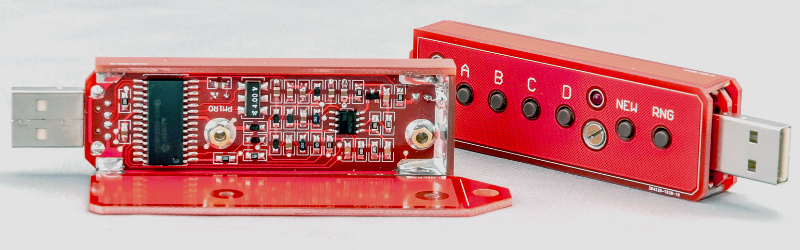
No, the sheets for those two red cases (password manager at the top and a small terminal next to the “Printed Conductors” headline) were made together with main PCBs by China supplier, as one panelized piece. The markings are in fact top silkscreen layer on the PCB. The lighter red areas are PCB copper polygon planes with 45° hatches. They feel very fine to the touch under the solder mask, like some strong thick textile, or so.
I’ve seen some tutorials on this before, but this one is quite extraordinary. It has been saved to my hard drive. Thank you, [Voja]!
I wonder if given a CNC router and a bit capable of making v-scores, you could apply tape to the back of the scores before snapping them, and easily fold up a box with perfect alignment. Essentially a version of the technique shown here:
http://hackaday.com/2015/05/15/smarter-than-wood-saw-blade-makes-perfect-foldable-joints/
It would not take into account the 2° caused by solder shrinkage, but I doubt that would prevent assembly, only cause a slight inwards bow of the walls. My first two PCB cases were made without knowledge of the 2°, but were still completed successfully, as the FR4 had enough flex to compensate.
Those 2° are not critical, you can also start from 90° and get acceptable box. By the way, the solder is soft enough to allow (very small) angle correction after it is cooled, if you apply strong enough force (but don’t try it, as you may damage it). If we are talking about FR4, the problem is the snapped edge, which is so rough and ugly that it needs good rasp treatment (you can see it on the upper photo in the “cutting” paragraph). Another thing is that one of two plate edges needs to overlap another one, which is infeasible if you don’t split them and treat the edges.
Sorry, now I visited your link and I see that there was the special saw used. Yes, you are right, it is a good point. Sorry for my wrong answer.
No problem, in fact you might have been right the first time. My use of that as an example might have been confusing, as it also demonstrates a particular wood blade and complex cut profile. I’m only suggesting a v-score, which could be cut with any CNC router and a common router bit. This short video on making a box from acrylic is a better example:
https://www.youtube.com/watch?v=OiETlYskTrY
And although I think it would produce a well-aligned and structurally sound box, I think you’re right in that it would produce rough and ugly looking outer edges. Though that wouldn’t be an issue for me, as I rarely leave the FR4 bare. Instead I usually sand, fill any large voids, paint, apply printed labels, and clear coat. Takes some time, but it’s acceptable for one-off projects.
I don’t have a CNC router to test this with, nor do enough of this kind of work to justify buying one yet. But I do have a project coming up with slate tile, for which I’ll need a small wet tile saw. I hear a diamond blade cuts PCBs easily, produces polished edges, and keeps the dust from floating around as well. Fairly inexpensive, and if it works as claimed, will make working with PCBs much easier.
It’s an excellent demo, worth keeping in mind. Yet, although it is very useful for some materials (wood, plastic, acrylic), there would be some problems for FR4 soldered joints. First, soldering iron will probably melt the glue on the adhesive tape, and the glass base in FR4 will shorten the saw life significantly.
You can make smooth on two sides polyester, epoxy or urethane fiber reinforced sheet fairly easily. First you need a piece of laminate or solid surface countertop more than 2x the size of the sheet you’ll be making. Cut it in half. If using laminate, apply a couple of coats of resin to the particleboard backing to seal out moisture.
If you want a smooth surface on the sheet, the countertop pieces must have a smooth surface. If you want a texture this will replicate into the sheet.
Get a can of TR-104 Hi-Temp mold release wax. Apply 3 or 4 coats, letting dry then buffing each coat. Follow the wax with any spray on mold release compatible with the resin you’ll be using. Another method is to use heavy polyethylene or polypropylene sheet, but any fold, wrinkle or other defect will be replicated in the resin.
Make several spacers the thickness you want the composite sheet. Wax them and spray on mold release.
Cut layers of glass, carbon fiber, hemp etc. to size. Mix and apply a layer of resin to one countertop piece then lay on the first fiber layer. Apply more resin in the center then add the next fiber layer. Don’t spread the resin out. You want the resin to squish from the center out, pushing air ahead of it through the fibers. Repeat until all the fiber you’ll be using is laid on.
Set the top countertop piece on and press down. Set heavy weights on top around the edges. C clamps will also work. Having this all level is important because any tilt will have it all trying to slide off. You’ll also want something to catch any resin that flows out. A slower curing, medium viscosity resin will work best, especially for larger panels. You want the resin to be able to flow out, while not curing so fast that any flex in the countertop pieces won’t have time to flatten. Too thin a viscosity will have the resin running out too much, leaving empty spots on the top side.
After the resin cures, drive wedges in to separate. Could also install T-nuts around the edges and use bolts for jackscrews, covering the bottom openings with packing tape to keep resin out of the threads. Could even use some through-bolts to clamp the form together.
How about an FR4 framed 3D printer where all the wiring to the motors, ends stops and other parts are etched onto the frame panels?
How about it?
Go build one
Mom always told us to never use solder joints for mechanical support
12 June 2015 from Perth, Western Australia
Greetings,
Just come across this web site, nice to see a great idea well carried to practical considerations, for what its worth I started out doing this many years ago in a narrow field more or less with an ‘open’ FR4 based structural product design with embedded through-hole with surface mount & have been selling an automotive based thermoset (wont melt at high underbody engine temperature) product for several years along the lines presented, which can be found on this link:-
http://niche.iinet.net.au
The offerings here however, have nicely gone beyond my very early approach & I have often thought about making a few demo products along similar lines to ideas presented here & pleased to see they have been carried off rather well.
So my congratulations for getting on & doing, reporting & offering it on a forum to discuss/pursue for the benefit of others.
With 3D printing taking off in all sorts of diverse ways, one can imagine all sorts of extensions which could well result in a type of finished product that appears so much more like “A bought one” ie With that higher end professional finish we would like to see & own which is indistinguishable from a commercial produced device as if from a production line process costing many millions to implement.
Many thanks & feel free to contact me as thoughts/developments arise. I am one of few who “Suffer from Enthusiasm” in that I have so many technical interests ensuring I am never bored even though the rare occasions occur when I talk to the only one listener present and have a “damn good” dialog only others who may likewise suffer can appreciate ;-)
Cheers
Mike Massen
Perth, Western Australia
eval(ez_write_tag([[300,250],’brighthub_com-medrectangle-1′]));.
It can seem like that, and it is best to be careful.
They can also detect and solve problems in your current
system.
I’ve been using 3mm and 6mm expanded PVC sheeting for my project enclosures for a while now. IMO, much less hazardous to my lungs with regard to dust inhalation.
Though I really like the idea of embedding stone of the circuitry into the case that FR4 allows.
I’m looking online for a good resource if this material. Any suggestions?
Don’t think I missed it but where can you get these pretty red PCB’s? Or any nice colour for that matter. The only ones I have ever seen in Australia on eBay, Jaycar, Altronics etc are dirty green or ugly brownish orange colour. Certainly nothing I’d want to be visible. Web searches don’t seem to show any results either?
I ordered them at http://accredologistics.com/
Scroll down to PCB online quote and you’ll see SM collors: Green / mate green / black / blue / red / white. I’lll try blue next time, they will probably be blue like the pot, but who cares :)
Why accept the base colour, ie What suggests only one colour was ever the issue, its not a model T (black), red is fine but, ANY colour is possible, even multi, even prints, its ONLY paint, whether 2-part epoxy or whatever, humans have had multicolors for millennia – no need to accept what someone tries to offer, its not a law etc ;-)
Here’s another fab house which provides color choices:
http://dirtypcbs.com/
Here’s a link to a photo of some yellow PCBs I had made from this place.
http://forums.parallax.com/showthread.php/157981-NonaProp-Inspired-by-TetraProp?p=1304332&viewfull=1#post1304332
I also purchased their solder stencils. Using stencils sure makes smt soldering a lot easier than doing it by hand.
I’ve seen other fab houses which offer different colors of PCBs. Itead Studio charges a bit more if the PCB isn’t green but not by a lot. I think Itead Studio also does a good job.
http://imall.iteadstudio.com/open-pcb/pcb-prototyping/im120418004.htm
If you want purple PCBs you can get them from OSHPark.com. These cost a bit more unless the board is small but the quality is great.
It’s a good idea to think about where the copper will be if the looks of the board is important. Some colors look very different when placed on top of copper compared with coloring the bare board.
The yellow on the boards I had made looked very different where there was copper compared to the places without copper. I think this could be used to one’s advantage and create a two tone look on a PCB.
BTW, I initially didn’t really like the look of the yellow boards I had made but the color grew on me with time. Now I like how they look. I think the main reason I choose yellow was because I hadn’t seen many yellow PCBs.
Very helpful, thanks heaps!
While cutting, sawing, drilling or sanding glass fibre based materials like FR4, use vacuum and mask.
Both with filtration either N99 or FFP3 rated.
Pulmonary fibrosis is very serious.
Most of those supplements work by stopping the cause of baldness.
In fact the height of a teenager increases dramatically.
Research strongly suggests that people with high levels of
Omega-3 fatty acids in their blood experience positive brain qualities
such as fewer signs of blood flow obstructions and fewer episodes of Dementia.
Lovely, like it.
I made my first FR-4 PCB based enclosure in 1977, hard to tell. It works out quite well till today, a shielded box for 2GHz RF measurement device with connectors, jacks, analog meter, 9V battery etc. It survived a lot, works and looks cool till today.
What is a mystery for me, who makes nice and reasonable silk screen and solder mask print on the PCB. Can you share?
I’ve used DirtyPCBs.com . They do a reasonable job. The alignment was dead on but plenty workable. I think I paid $25 extra for a stainless steel stencil (several years ago).
Most fab houses include silk screen (I think it’s really ink jet).
I’ve used Itead Studio: https://www.itead.cc/open-pcb/pcb-prototyping.html
I thought they did a good job.
I think Seeed has a fab service but I haven’t used it.
OSHPark.com makes nice purple PCBs but they’re kind of expensive compared with some of the other places. I use OSHPark for small PBCs since they change by the square inch and I can get three small boards delivered for a few dollars.
Do you have your 1977 enclosure documented anywhere? It would be fun to see.