Despite the existence of FPGAs and CPLDs, there’s still a necessity for very small programmable logic devices. GALs, PALs, and other old tech just won’t cut it, though, and so we are left with a new generation of programmable devices that aren’t microcontrollers or CPUs. The GreenPAC from Silego fill this niche quite nicely, with the ability to implement counters, ADCs, logic glue, level shifting, and comparators in a single chip. For any homebrew electronics tinkerer, these devices have one very obvious problem: they’re really, really small. The smallest GreenPAC device has 12 pins stuffed into a 1.6 x 1.6mm QFN package. You’re not hand soldering this thing.
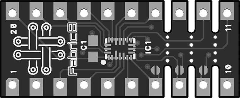
For [Nick Johnson]’s Hackaday Prize entry, he’s taking these small programmable logic chips and making it easy to create your own custom ICs. Basically, it’s a breakout board for GreenPAC devices that stuffs these tiny chips onto a much more reasonable DIP package.
Breakouts aren’t enough, and to program these small chips, [Nick] is also building a board based on an ARM microcontroller. With USB input, a way to generate the 7.5V used for programming, and a breadboard friendly format, this programmer will tell these tiny chips what to do.
Not many people are building stuff with PALs and GALs anymore, but there are still a lot of work that can be done with small programmable chips. There’s certainly a place for tiny programmable logic chips like this, and anything that gets them in to the hands of more people is okay in our book.


Semi-important clarification: it’s GreenPAK (with a K). And presumably this is the GreenPAK 4 (http://www.silego.com/products/greenpak4.html). It’s an unusual chip, to be sure. And it’s…one-time programmable? There’s something I haven’t seen in a while.
Strictly speaking, would a tinkerer really want a one-time programmable anything? Final product…? Yeah, I can see that but a hobbyist or a tinkerer going through dozens of iterations and recycling project parts? No….
they are 60 cents each!!!
way cheaper than all the TTL PROM’s I stuffed up back in the day!
With today’s brute force programming methods, that’s going to add up fast.
The modern “hacker” or rather, the maker, doesn’t bother to figure out how things should work. They’ll just put something together, see if it works, and change it if it doesn’t. That’s why people use Arduinos for light switches.
Thank you for that level headed response.
In addition, I’ve come across lots of poor documentation that mentions you can do X without telling you that W is a necessary step. Or worse, the necessary information has spread across a ton of different references and every single one is on a different revision. I spent hours this past week puzzling over an API with an obscure call with hundreds of tests trying to get it to work because the damn documentation was so vague.
That’s why I’m fond of the AVR line. One or two documents for the family and a single monalithic document for a specific uC.
You just have to get better in reading multiple documentation at the same time. That’s a useful skill to have.
Most of the chips I use usually have 1 datasheet for the hardware with actual performance specs and a separate programming manual. There might be additional app notes with source code examples for a particular peripheral. Sometime I have to look up the actual ARM documentation if I want to see the NVIC or some ARM specific stuff not covered. I would expect you have to do that for Atmel too.
I don’t believe in brand loyalty. Whoever has the best chip for *my* money get designed in. My HaD projects are kinda funny as they are tagged under different vendors.
How many iterations do you normally do before you release a prototype ?
How many iterations do you normally do before you release a product ?
How many field changes do you normally do before you release to marketing ?
This is a business model to keep cash flow high.
Nice to know someone still uses 1980s technology and business methods.
Yes, I’m sure their eeeevil business plan is to make 60c off you each time you iterate a design on your workbench.
Even on a good day when I simulated the logic and have everything mostly working before burning a chip, I think I can easily go through 7-8 tries because I change my mind on the hardware specs or added more features.
Not seeing any major cost saving at all for low volume production if the parts have to be discarded because of wrong or out of date firmware. Are they just saving some minor chip space – charge pump and transistors for OTP vs FLASH?
That’s why you can run it in ’emulated’ mode on the programmer, to test things out without committing the design.
My other goal is to have a large library of prebuilt designs for common tasks, including pin-compatible replicas of many 7400 series ICs.
You simulate the chip to see if it works before you program it. Plus they are dirt cheap. Have you never heard of glue logic?
GreenPak3, actually – the 4 are harder to program and less well documented, so I decided to stick with the better-documented 3.
They’re one-time programmable, but they have an ’emulation’ mode in which you can program the SRAM, which they retain as long as they have power. I’m building the programmer board with that in mind; it will have 0.1″ pins on the bottom to plug into a breadboard, allowing you to prototype designs on the greenpak without using up a device. Besides that, the goal is to get the price for individual breakouts so low that you don’t mind using up a couple.
Ah, thanks, the emulation mode is something I missed. That makes a lot more sense for development. And while I struggled to understand the point to the chip for a while, at tha size and price point, it can replace power up logic, which is actually useful for me on one of my work-related projects. Being able to compress some normally more discrete logic on the board is always good in my book!
One suggestion… breakout to SOIC, not DIP. DIP is great for breadboarding, but being OTP parts….
And besides SOIC to DIP adapters are staple components for prototyping. For any final product, SOIC is likely what you want.
Duh… by SOIC, I really meant “castellated” to fit in a SOIC footprint
I considered it, but SOIC isn’t as prototyping-friendly. See my post above for the development methodology I had in mind.
Also, if we are talking prototyping, they sell a socketed adapter board for $20
http://www.silego.com/buy/index.php?main_page=product_info&cPath=56&products_id=331
Unfortunately, that’s intended to adapt ICs for use on their programmer board; it breaks out to a 2 x 0.1″ header, so you’d have a hard time using it on a breadboard.
OTP programmable parts. What real prototyping are you going to be doing?
JMO, but packaging it in a final-product friendly package that can be hand soldered would have more value.
If I going to be breadboard prototyping, I would just buy their adapter and adapt it to breadboard friendly.
You are thinking about prototyping a circuit where this is just a component of it. But what about after the prototyping?
And again… SOIC to DIP already exists for prototyping needs.
I would revisit the SOIC concept again.
As I said above, the devices have an “emulation mode” in which only the onboard SRAM is powered, allowing them to be used to prototype without programming permanently. Either way, a prototyping cycle that involves soldering and unsoldering parts from a PCB isn’t a particularly friendly one.
Additionally, I’m not even sure it’s possible to make a castellated PCB that fits in a SOIC footprint; I certainly haven’t seen one.
A hand-production-friendly form factor is certainly worth considering for the future, but right now my focus is on making it easy to achieve simple tasks with these devices, such as replacing 7400 logic.
“Additionally, I’m not even sure it’s possible to make a castellated PCB that fits in a SOIC footprint; I certainly haven’t seen one.”
SOIC-W (wide body) can be found in 5-10mm wide. A SOIC-W-16 for example is 7.4-7.6mm wide. I have used the universal SOIC adapters before to tag down castellated bluetooth modules. It lines right up with the castellated pins.
The objections you have made don’t really explain why not. Nothing prevents someone from making easy modification to the $20 socketed adapter for breadboard prototyping. You even made the adapter if you just reversed the gender of the connectors. But again, what is the user to do when they want to actually integrate the part into their final board? Are they going to stick 14 of these huge DIP boards in their final project?
I’m not telling you how to do your project or criticizing it. Just offering feedback in what I think many would find useful.
As I mentioned earlier, the devices support an in-SRAM ’emulated’ mode; that doesn’t work if your prototyping process involves powering it down and plugging it into a breadboard, so you end up having to throw away a device for each trial. Plus, you have some enormous adapter-plus-jury-rigged-breadboard-converter sticking up out of your breadboard.
For production, I expect users will either use the DIPs directly (if they’re building a DIP circuit, or they’re selling kits, or they’re just making a couple for themselves), or they will switch to the raw package once they’re done with prototyping, and have a professional assembler (or someone with a stencil and time on their hands) put them together. The market in which people want a smaller-but-not-that-small package to solder onto a production PCB seems narrow, especially compared to the large number of people who could be playing with these but aren’t because there’s no good prototyping/experimenting story currently.
If you have 14 of them, you should probably just be using a CPLD.
I am not going to keep arguing with you. What’s the point? It’s your project.
But, yes, I heard you the very first time you mentioned the RAM mode. I even read it in the article before you mentioned it. You emulate until you get what you want and then you program it permanently for your final design. You are going to have to remove power from your breadboarded adapter to put it on your final board, aren’t you?
I am not trying to pick on you, but you are so invested in the way you are doing it, your arguments are not logical.
Have a good day and good luck
No – the programmer accepts a breakout board in a socket, and itself fits onto the breadboard. You program it while it’s on the breadboard, then you can test it without removing power or moving the device physically.
I’m open to suggestions and criticism, but I think I’ve provided cogent arguments why I don’t think a SOIC breakout is as useful as the DIP format I’m currently working on. The fact we disagree does not mean I’m exhibiting commitment bias or am otherwise being illogical.
ok
I think what our friend Justice_099 is asking is, when the DIP form factor is done, could you look at creating a SOIC version too? I have some applications where I’d like SOIC, and some where I’d prefer DIP.
Anyways, great work.
Yes
It’s certainly on my list to consider. It’d be sufficiently different from the DIP breakouts that it might be easier to just make an adapter for the official dev kit rather than make it work with the Fabric8 programmer, though.
The routing and mousebites on the bottom of the fabric8 breakout are set up so that you can turn your breakout from a 20-DIP into an 18, 16, or 14 pin one by snapping the end off and soldering a GND jumper, and the pinout is designed to match common 7400 series logic ICs. That’d be both harder and less useful in a SOIC format breakout – and the programmer’s ability to plug into a breadboard wouldn’t be nearly as useful either.
That said, a custom adapter for the official dev kit is much easier than the custom programmer – I’ve already got one for alpha testing of the fabric8 breakouts.
I have seen the Japanese uses a castellated pins design to put a FPGA/CPLD into PLCC form factor PCB. It is the best of 2 worlds, you surface mount the PCB or use a PLCC sockets that fits on proto boards or even a wire wrap board.
1.6mm x 1.6mm QFN is not much more difficult than a SOIC if you already
ave a PCB – even one from a Chinese PCB shop. I have reflow a few QFN now and even remove and reflow the same part a couple of times,
I like the QFN better as it is smaller and you don’t have to worry about bent pins. Reflow is just a hot air tool away. Thanks to cheap Chinese tools, they are now even some with a regular solder iron.
If you are going to use SOIC why use a breakout at all? I would consider getting one of these for breadboarding. Not sure what to so with an SOIC version though.
QFN without thermal pad is not so difficult to solder, as long as the pads go up the side. Just run a blob of (good quality) tin along the edge of the part.
The point is that the entire part is 1.6mmx1.6mm. I assume that means the pitch is quite tiny. I know the technique you are referring to but you are not going to accomplish that with any confidence without a very good scope. You also need good flux for that technique and zero moisture (pre-baking board, solder, and part) because even the tiniest solder-ball will likely create a short.
The package is actually STQFN. The pitch is .4mm. The pads do come up the sides at .15mm nominal.
My finest iron tip is 1/3 the size of the entire part.
http://www.silego.com/uploads/Products/product_275/SLG46120r100_05262015.pdf
I’ve done quite a few QFN parts with 0.5 mm pitch by hand, with a 0.8mm tip on the iron, and some cheap drugstore +3 reading glasses.
Because the pads are so small, it’s very hard to get bridges between them, and even if that happens, they’re easy to clean up by running a clean iron along the edge. I actually find them easier to solder than 0.5 mm LQFP, which are much more sensitive to bridging.
.5mm != .4mm, STQFN != QFN, And you are not talking about 1.6mm x 1.6mm parts. Take a ruler and see just how small that actually is.
I know it’s cool to brag around here but the audience is generally experienced enough to know better.
No, 0.4 mm is a little smaller than 0.5 mm. But 1.6 mm is pretty easy to handle. It fits nicely in a pair of tweezers, so it’s easier to handle than some 6×6 mm QFN, and not nearly as small as a 0.5mm wide 0402.
And the point is not to brag, but to have people overcome their irrational fears of surface mount components.
Well, ok then. Why don’t you get these parts, write up an article, and show all us incompetent people?
Until then…. *shrug*
No, you should try it, and discover that it’s not as hard as you think it is.
I am an electrical engineer with nearly 20 years of experience. No fear of SMT here. I’m just realistic.
But whatever.
I have also hand soldered QFN packages, 0.5mm CP2502 UART Bridges to be specific, with a 3mm chisel tip and as long as you design your footprint with enough opening on the solder mask you could probably solder it with a solder crayon.
The trick is use plenty of flux and a good set of tweezers.
I use a $3 loupe to see my results.
also an ee.. dont fall into the trap of putting self imposed blinders on based in your interpretation of reality.
ok
I have hand reflow 0.5mm QFN parts and even smaller packages like 0.4mm CSBGA with just a flash and cheap magnifying glass. Also worked with 0.8mm x 0.6mm resistor array, 1.0mm x 0.6mm transistor (DFN1006-3).
It just takes time.
For anyone interested, I already have some breakouts and a few adapters for the official dev kit, and I’m looking for a very limited number of alpha testers. You’ll need to have your own Greenpak3 dev kit, but I’ll send you everything else – all I ask for is feedback. Email me at nick@arachnidlabs.com if you’re interested!
Woooo! They have OSX and Linux designer softwares and not just Windows…
I’d LOVE to play with the collection of PAL and GAL chips I have, but there are no open hardware/software tools for them (for linux, I’m not paying to build a windows machine just to do it)
The industry seems to want to keep the programming methods a secret.
I have a collection, I’m waiting…. one day the info will come out and I’ll be able to use an arduino based programmer.
Fun fact – the bitstream for Greenpak devices are documented in the datasheets! On my (very long) todo list once I’m done with the hardware is to build an opensource toolchain of some sort for them.
There are some open source GAL programmers and PAL assembler source code in C out there. I build a GAL programmer with just the programming specs from National Semiconductor back in school day. Got to watch out though, there are a lot of other chips out there are are not compatible with the programming.
Go play with CPLD, they are a lot nicer and the vendor have JAM player source code available if you want to bit bang the JTAG programming.
This is a really clever idea, placing this device in a breadboard/socket-friendly DIP package, even with breakaway pins to ensure it fits in a variety of package sizes. In terms of tinkering with programmable logic, it sounds complementary to Colin O’Flynn’s great Bora Board — perhaps learn on the Bora, then implement permanent designs on this?
BORA looks pretty cool! Part of the goal here is to allow you to do tinkering and development on the programmer, by plugging it into a breadboard and running in emulation mode – so you don’t have to burn a device to test out each new design.
Not a huge amount in it, what about these little fellas?
http://www.microsemi.com/products/fpga-soc/fpga/igloo-nano
Full FPGA, reprogrammable, on board flash, only 3mmx3mm….
If only I had a use for one….
Oh, those look very cool indeed. Pity they’re only low voltage (1.5v).
Thats the core voltage, you can have I/O up to 3.3V
I really love PSoC 5LP for configurable Logic cells and CPU (Cortex-M3) in single one package with Flash.
Lattice MachXO2 in 25-ball 2.5mm WLCSP appears to be a bit more usable (it has hardened SPI, I2C, Flash, block RAM, RC oscillator and PLL except for the very small devices). These devices might be an option for slightly more demanding tasks.
I find my self using a large number of 74s or a cheap cpld where this would fit perfect!
Silego – might not run Crysis but one could make a solid call out to a single step 8-64 bit fixed point ALU(?).
Haven’t read the specs but IF the speeds close can get close to the 90’a 7400’s might be decent. Of course probably not great to compare to backplane for ECL’s/PECL’s.
Nice project to make it these Greenpaks easier to use though!