Microchips and integrated circuits are usually treated as black boxes; a signal goes in, and a signal goes out, and everything between those two events can be predicted and accurately modeled from a datasheet. Of course, the reality is much more complex, as any picture of a decapped IC will tell you.
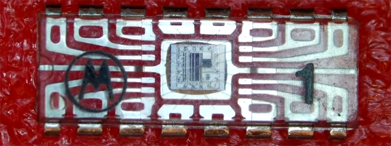
[Jim Conner] got his hands on a set of four ‘teaching’ microchips made by Motorola in 1992 that elucidates the complexities of integrated circuitry perfectly: instead of being clad in opaque epoxy, these chips are encased in transparent plastic.
The four transparent chips are beautiful works of engineering art, with the chip carriers, the bond wires, and the tiny square of silicon all visible to the naked eye. The educational set covers everything from resistors, n-channel and p-channel MOSFETS, diodes, and a ring oscillator circuit.
[Jim] has the chips and the datasheets, but doesn’t have the teaching materials and lab books that also came as a kit. In lieu of proper pedagogical technique, [Jim] ended up doing what any of us would: looking at it with a microscope and poking it with a multimeter and oscilloscope.
While the video below only goes over the first chip packed full of resistors, there are some interesting tidbits. One of the last experiments for this chip includes a hall effect sensor, in this case just a large, square resistor with multiple contacts around the perimeter. When a magnetic field is applied, some of the electrons are deflected, and with a careful experimental setup this magnetic field can be detected on an oscilloscope.
[Jim]’s video is a wonderful introduction to the black box of integrated circuits, but the existence of clear ICs leaves us wondering why these aren’t being made now. It’s too much to ask for Motorola to do a new run of these extremely educational chips, but why these chips are relegated to a closet in an engineering lab or the rare eBay auction is anyone’s guess.


Can anyone in the business make an educated guess what a small-ish run (couple thousands maybe) of something like this would cost to make nowadays?
It would probably be cheaper in the end to just buy the dies from the manufacturer and get yourself an old wire bonder (pretty easy to come by). You could break out to a custom made PCB in lieu of the epoxy package. Drop a blob of clear epoxy on top to protect the bare wires.
I have seen 40 pin ceramic dip packages without ICs in the center well, I wonder if these are commercially available.
I am pretty sure it would be silly expensive to get a short run of clear packages done. I know companies make them, I have (somewhere) a DIP-8 light sensor in a clear package.
They are about 25 years old and I would say that the plastic is the same price but the cost of stopping a run to change the encapsulation glop would be vast…they did these as a special run al those years ago and we are still using them so they are hardly a big seller
Seeing how it’s Motorola it’s just a case of pulling out a spare extruder and getting clear plastic they probably already use else ware
Exactly but I would imagine it would be a new batch since after 25 years it’s probably gone off. Also stopping a machine doing millions of chips to do comparatively few clear ones would be the most expensive thing as well as the following clean down of the machine etc
Specialized plastic encapsulation of microchips is not ‘pull out a spare extruder’ type of process.
Likely they would have to stop a line – also, ‘opaque epoxy’ implies a chemical-set plastic, it is totally possible the high heat of injection molding thermoplastics will destroy the die – though clear epoxies are readily available.
I would imagine buying the chips on substrate, wirebound, then figuring out a low volume encapsulation might be viable.
All epoxies are thermoplastics, not thermoset. But otherwise, yes.
You got that backwards: epoxies are thermoset. Thermoplastics melt and can be remelted — usually they’re formed with heat. Thermosets undergo an irreversible chemical reaction and don’t readily remelt — like 2 part epoxy.
Designing a custom chip would be expensive but a wafer has many chips. As a design engineer we would just purchase a tested wafer if a package size we required was not available and package it ourselves.
You have it right,Vic, From the site http://www.nutshell-videos.ed.ac.uk/les-haworth-teaching-chips
“fabricated using technology that is not leading edge so the devices are very large compared to modern state of the art circuits”
“Chip 1 simply has resistors fabricated from either aluminium or polycrystalline silicon. Chip 2 has only MOS transistors of different sizes allowing simple logic gates or analogue circuits to be constructed. Chip three has diodes and photodiodes while chip 4 is the only chip with more complex circuitry including a ring oscillator that allows an assessment of the delay introduced by a single logic gate.”
These are custom chips specially designed ror their purpose and not simply standard chips that have been encapsulated in transparent plastic.
Still available from here in the UK: http://www.mindsetsonline.co.uk/Catalogue/ProductDetail/semi-conductor-teaching-chips?productID=56c87490-a077-420a-89ca-e78eb155d758&catalogueLevelItemID=3c05c2fe-42b0-4c4a-a996-7d3e85b75b73
Great one…. Jim’s a mate of mine and spends a load of time on his vids. the hydroponic ones are particularly interesting!
Those chips are generally available if you look in fact I bought a set about 5 years ago with a similar idea …need to dig them out :)
From memory, some circuits are light sensitive, so they need to be in opaque containers.
Eg. https://www.raspberrypi.org/blog/xenon-death-flash-a-free-physics-lesson/
All integrated circuits are light sensitive, just a matter of how much it impacts performance.
I would guess it’s more than one would expect, especially considering most of us have only ever had to deal with the regular kind. And this would let a LOT more light in than simple letting it leak under the chip around the ball array. It might work quite well now in a black epoxy chip….but you never know what you’ve got until it’s gone. I very much doubt anything with a large degree of complexity can be built this way without it being turned into a quivering pile of bit-flips. (especially CPUs and RAM)
Awesome – I got featured on hackaday :-) … I just wanted to add that I’m working on videos for the other three chips too which will be hitting YouTube in the next few weeks. Thank you Brian Benchoff for sharing this video with hackaday. Cheers!!
Won’t the light affect all the transistor junctions?
yes, all transistors are basically opto-transistors ..That’s why they have black chips, also why the RPI crashed under strong light which got through the really thin plastic of that little chip.
Another good read :)
https://www.youtube.com/watch?v=VhsCcR7YEXI
These are very cool. I still have some decapsulated parts from when I was a failure analyst at Motorola and will sometimes show them to kids under the microscope. It is pretty easy to decapsulate an epoxy part if you have a vent hood. Here’s how we used to do it: We had a Dremel-like mill mounted on what could have been a Dremel drill press attachment. We’d remove epoxy mechanically (but not too deep) to form a cavity in the chip. You don’t want to go too deep or you will clip the bond wires, but if you go very shallow, it will take a long time for the next step to finish.
Once you have the cavity, you put the device on a hot plate. We had little copper bars that would sit on the plate and the DIP package would straddle the bar so the bottom of the device would get hot. I don’t remember the exact temp but I’m guessing make 100F. Then you carefully put fuming nitrate in the cavity. After awhile, you take the device (careful, it is full of hot fuming nitric) and rinse it off with DI water and alcohol (two rinses). If the die isn’t exposed (or is partially exposed), you put it back on the hot plate and use more fuming nitrate.
Now getting the passivation (the glass top layer) off is way worse, requiring nasty HF. But for just optically looking at the die, that’s all you need is heat, fuming nitrate, and a dremel. I have heard that since hackers have issues getting and handling fuming nitric you can use heated up nitric, but I’ve never done that.
Sometime back in the mid 1980s the local university engineering dept had a huge “science fair” and some chip manufacturer – probably either Moto or Intel – was giving out silicon wafers that were pulled just before they were sawed into chips. They also had visible ICs as used in this article – iirc 40 pin DIPs. I think I still have mine back home.
There are also EPROM microcontrollers with windows on top just like those old EPROMs.
EPROM chips can be used as very poor photovoltaic cells. Just connect a lot of them in series with power and ground then expose to bright light.
Here’s Video number 2 in the series :)
[youtube http://www.youtube.com/watch?v=F-D6xzllrno&w=560&h=315%5D
Think it was the old Kodak Ektralite cameras that had a clear light sensor IC inside
Recently picked up a clear SOIC photodiode with built-in amplifier, good stuff.