In the previous installment, we talked about why flip flops are such an important part of digital design. We also looked at some latch circuits. This time, I want to look at some actual flip flops–that is circuit elements that hold their state based on some clock signal.
Just like last time, I want to look at sequential building blocks in three different ways: at the abstraction level, at the gate level, and then using Verilog and two online tools that you can also use to simulate the circuits. Remember the SR latch? It takes two inputs, one to set the Q output and the other to reset it. This unassuming building block is at the heart of many other logic circuits.
 A common enhancement to the SR latch is to include an enable signal. This precludes the output from changing when the enable signal is not asserted. The implementation is simple. You only need to put an additional gate on each input so that the output of the gate can’t assert unless the other input (the enable) is asserted. The schematic appears on the right.
In the case of this simulation (or the Verilog equivalent), the SR inputs become active high because of the inversion in the input NAND gates. If the enable input is low, nothing will change. If it is high, then asserted inputs on the S or R inputs will cause the latch to set or reset. Don’t set both high at the same time when the enable is high (or, go ahead–it is a simulation, so you can’t burn anything up).(Note: If you can’t see the entire circuit or you see nothing in the circuit simulator, try selecting Edit | Centre Circuit from the main menu.)
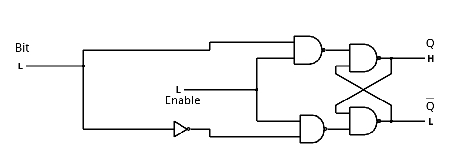 The SR latch could be useful, but in many applications it is inconvenient to have to expressly set and reset it. I said last time, these circuits were like a memory bit, so how could you make the latch just remember the state of a single bit? It’s easy. Just drive the S input with a bit and the R input with the inverse of the same bit. The diagram to the right is in falstad or using Verilog.
This is practically a digital version of a sample and hold circuit. When enable is asserted, the output follows the input. When enable is not asserted, the output holds its value.
There are other ways to get the same effect. Because latches and flip flops are so universal, there are a variety of designs. For example, look up Earle latch, which offers a fixed propagation delay compared to the traditional latch design.
The D Flip Flop
The SR latch modified with the inverter is often called a D latch because the single input is data for the latch to store. To make it a D flip flop, though, you need to arrange to capture the data at a clock edge, not just any time the latch is enabled.
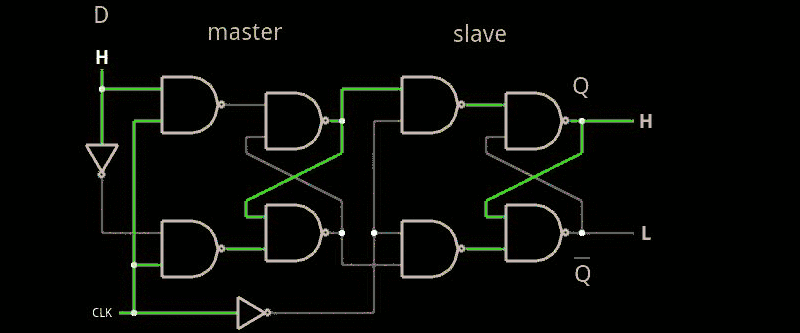
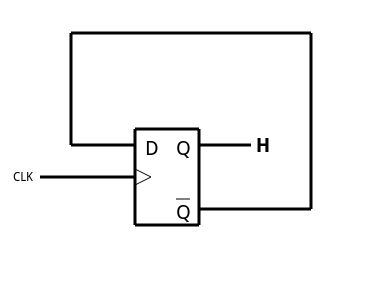
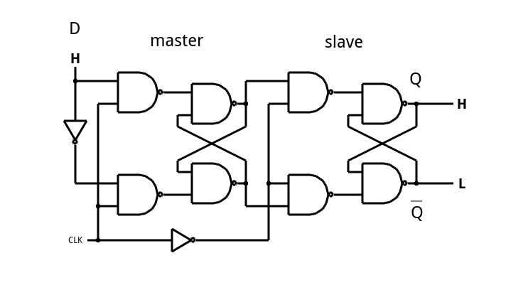 One way this is done is called a master slave flip flop (which doesn’t have to be a D flip flop). The idea is to cascade two latches with a single enable line. However, the first flip flop (the master) gets the enable line straight. The slave gets an inverted copy. What this means is when you enable the flip flop, the master’s output will track the input. However, since the slave is disabled (because of the inverted enable line), no output change will occur. When the enable line drops, the master will hold the last state it saw, but now the slave’s enable line will turn on and the output will change. Since the master’s input can’t change, the effect is the entire flip flop stores the state of the input at the time the enable line is deasserted. Here’s a simulation (see image to the right).
It is more common, however, to make flip flops sensitive to the actual clock edge. One simple way to do that would be to use the pulse edge detector I mentioned earlier to feed the enable output of a conventional latch. The simulator also shows a different method using a few latches, one of which is built with a three-input gate.
In Verilog, edge sensitive flip flops are easy to create. The synthesis tool takes care of the details. Here’s an edge sensitive D flip flop:
module dff(input clk, input d, output reg q, output qnot);
assign qnot=~q;
always @(posedge clk) q<=d;
endmodule
That’s it. You might add a reset signal:
module dff_reset(input reset, input clk, input d, output reg q, output qnot);
assign qnot=~q;
always @(posedge clk)
 if (reset) q<=1’b0; else q<=d;
endmodule
In this case, the reset is synchronous because it only happens when the flip flop is processing a clock edge. One of the EDA Playground examples shows a D flip flop with an asynchronous reset you can experiment with.
The T Flip Flop
 A T (or toggle) flip flop changes state on each clock pulse (at least, on each enabled clock pulse). This is simple to accomplish if you have a D flip flop. Just connect the inverted Q output to the D input (see left) and you are done. Notice this has the effect of dividing the clock frequency by two, and that’s one thing you frequently use flip flops for: frequency division.
In Verilog, the T flip flop is very simple (although you could, I suppose, wire up a D flip flop, it isn’t necessary):
module tff(input reset, input clk, output reg q);
always @(posedge clk) if (reset) q<=1’b0; else q<=~q;
endmodule
There are many other ways to build a T flip flop, including by wiring the J and K inputs of a JK flip flop together (see below).
The JK Flip Flop
The JK flip flop sounds mysterious, but it really isn’t. Think of it as an SR flip flop where the J input is equivalent to the S and the K input is equivalent to the R. The reason it is not an SR flip flop is that it has well-defined behavior if you assert both inputs at once: the output toggles (like a T flip flop).
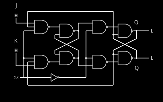 You can find a simulation of the JK flip flop and experiment with it (see image to the left). Note the simulator has a metastability problem (see below) loading the JK flip flop from a link. If the Q output oscillates, go to the Circuits menu and under Sequential Logic, select Flip Flops, and then JK Flip Flop.
In Verilog, you usually don’t model this directly, although you certainly can. Here’s a Verilog JK flip flop:
module jkff(input clk, input j, input k, output reg q, output qnot);
assign qnot=~q;
always @(posedge clk)
 case ({j, k})
 2’b00: q<=q;
 2’b01: q<=1’b0;
 2’b10: q<=1’b1;
 2’b11: q<=~q;
 endcase
endmodule
A Little More About FPGAs
Much of the time you don’t directly write flip flops by themselves when coding for an FPGA. First, most FPGA vendors supply optimized flip flop macros that you can use that take advantage of on chip resources. In addition, you’ll usually code at a higher level and the synthesizer will infer the flip flops you want.
For example, you might write a simple state machine:
 always@(posedge clk or posedge reset)
 begin
   if (reset)
   begin
     state = s1; outbit = 1'b1;
   end
   else
   begin
     case (state)
 s1: begin
     if (x1==1'b1) state = s2;
     else state = s3;
     outbit = 1'b1;
     end
 s2: begin
 . . .
   endcase
   end
 end
Even though that doesn’t look exactly like one of the examples, the FPGA synthesizer will recognize this and build the corresponding circuit using flip flops. It also recognizes other flip flop-based circuits like counters and shift registers.
That’s not to say you shouldn’t know the flip flop types and know how to code them. Being able to do so will help you understand what the tools are inferring for you. However, if you look through a lot of practical code, you won’t see many exact copies of these flip flop instantiations.
What you will see, though, is clock sensitive always blocks with assignments in them. You’ll also see higher level constructs like counters and state machines that use these building blocks internally.
Flip Flop Timing
In the first part of this series, I talked about how our neat schematics don’t match the real world and while that is sometimes a problem, it is also sometimes a good thing. Flip flops are no exception. Because of real world circuit elements, flip flops have several issues: setup time, hold time, and–more generally–metastability.
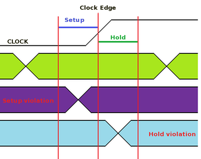 You can see a graphical representation of setup and hold time to the left. Inputs to the flip flop must be stable for the setup time before the active clock edge. The inputs also have to stay stable for at least the hold time after the clock edge. Graphically, then, the signal can’t change between the outer red lines. The green signal is legal, but the other two violate the rules. In practice, this limits how fast the clock can be. Suppose your click has an active edge every 10ns. If your combinatorial logic feeding the flip flop has a 9ns delay, that should be ok, right? Not if the minimum setup time is more than 1nS. Setup and hold violations are sometimes difficult to troubleshoot, although modern scopes sometimes have special trigger modes to find violations.
If you violate the setup or hold times, the flip flop may go metastable. What this means is the flip flop may behave badly. In some cases it will oscillate or it may take longer to change states than normal. There are several cases where you have to worry about metastability. One is when you are changing clock domains (that is, feeding a flip flop from another flip flop that uses a different clock). Another problem is when you have data coming from a purely asynchronous domain such as a user input switch or an RS232 port. In that case, there’s no way to be sure the input won’t change within the setup or hold time (or even right on the clock edge).
When you have an asynchronous input you’ll usually cascade it through multiple D flip flops. Each additional flip flop you use reduces the chance of metastability (at the output). However, it also delays the input by a clock cycle for each flip flop.
Metastability is a big topic and probably deserves a whole post in its own right. If you can’t wait for that, there’s a good IEEE paper on the subject or have a look at the video below.
There are metastability resistant flip flop designs that have a reduced chance of going into the metastable state. These aren’t perfect, though, because you can’t make both the setup and hold times zero. In the end, there’s no substitute for good design.
Wrap Up
Flip flops are a powerful tool for a digital designer’s arsenal. Implementing them can range from a 555 chip (no kidding, you can make a slow flip flop with a 555) to using discrete components, to using ICs to writing Verilog or VHDL. Learning about flip flops is a lot like learning about chess. You can learn the moves in a few minutes. You can spend a lifetime trying to master them. I hope these two posts have taught you the moves. The rest is up to you.


Nice
When implemented on an IC, do flipflops still have the structures as shown, or is the gate’s logic merged/remapped into an equivalent circuit?
I guess what i am trying to say is are these models accurate, or just another layer of abstraction hiding a different CMOS implementation?
That’s a great question and as far as I know the answer is: it depends. First, it depends on what level you are looking at. Vendors like Xilinx and Altera generally deliver macros for these flip flops that map to their cell structure, so from that level, the answer is yes you can ask for a jkff macro and get what you see here.
However, at the die/cell level, they are probably implemented differently to save real estate, match the silicon attributes better, and other reasons. They probably also take a two-phase clock or rely on other “strange” behavior because they can. Also, the flip flops will be configurable, so they will incorporate transmission gates or muxes or some other way to “wire up” the naked flip flop logic into the different kinds of configurations required for the various macros.
Of course, everyone could do it differently and there might be some on die flip flops that look exactly like the ones presented, but usually you’ll see inverters with feedback controlled by some kind of transmission layout (a dynamic flip flop). For example, look at this: https://www.semiwiki.com/forum/content/2494-your-synchronizer-doing-its-job-part-1-a.html (the article is a bit arcane, but look at the dynamic flip flop implementation at the top). Then again, this article (http://www.design-reuse.com/articles/37799/configurable-asynchronous-set-reset-flip-flop-for-post-silicon-ecos.html) shows some flip flops with more traditional gate structure. Here’s a good academic-type paper about different topologies: http://www.ijert.org/view-pdf/10123/design–implementation-of-embedded-logic-flip-flop-in-180nm-technology. Unless you are doing chip layout, you really don’t need to read this, but it is still interesting (I used to do the opposite: tear ICs apart to determine why they failed for a Very Big Company). Some layouts are smaller, have better fan out, lower power, etc.
The tsmc gate library is probably visible enough to see how they implement different flip flops if you are really interested. Usually, when you see a vendor’s cell it will show a schematic like we’ve looked at. For example, https://courses.cs.washington.edu/courses/cse467/03wi/FPGA.pdf has some Xilinx 4000 cells (old stuff) and you can see there are two D flip flops plus a lot of muxes and stuff to configure it.
Great question. If I didn’t quite hit the answer, ask again.
Al, I know you’ve discussed asynchronous and synchronous signals but I note in your examples above you appear to jump from having a purely synchronous reset (synchronous assert and de-assert) to an asynchronous assert with synchronous de-assert behaviour which I don’t think you’ve explicitly discussed the “whys and wherefores” (there are good reasons why ASIC design is typically done using the latter which you skirt by in your discussion on setup-and-hold issues).
Hi Sheldon. Well I did mention that one was async and one was sync, but I didn’t get into it much more because a) it was running long, and b) as you point out, it is a different set of trades based on your medium so there’s not one “right” answer for everyone. On most (but perhaps not all) FPGA fabric, synchronous reset is “better” because you avoid metastability and the (frankly) the tools hate analyzing large fan out async signals (or, at least they used to; maybe they are better these days). A good paper on the subject for anyone interested: http://vlsi.pro/synchronous-asynchronous-reset/
I did, however, want to show both.
Gratitude it’s a great deal