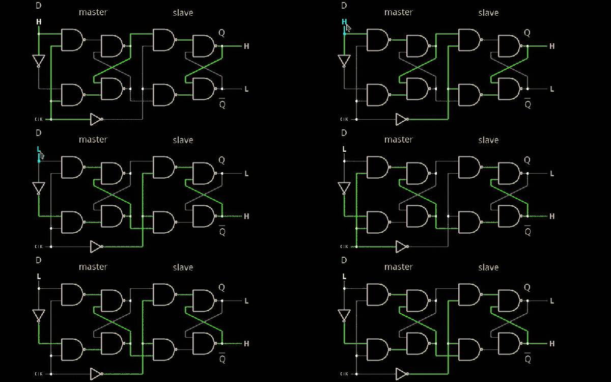
In the previous installment, we talked about why flip flops are such an important part of digital design. We also looked at some latch circuits. This time, I want to look at some actual flip flops–that is circuit elements that hold their state based on some clock signal.
Just like last time, I want to look at sequential building blocks in three different ways: at the abstraction level, at the gate level, and then using Verilog and two online tools that you can also use to simulate the circuits. Remember the SR latch? It takes two inputs, one to set the Q output and the other to reset it. This unassuming building block is at the heart of many other logic circuits.
 A common enhancement to the SR latch is to include an enable signal. This precludes the output from changing when the enable signal is not asserted. The implementation is simple. You only need to put an additional gate on each input so that the output of the gate can’t assert unless the other input (the enable) is asserted. The schematic appears on the right.
In the case of this simulation (or the Verilog equivalent), the SR inputs become active high because of the inversion in the input NAND gates. If the enable input is low, nothing will change. If it is high, then asserted inputs on the S or R inputs will cause the latch to set or reset. Don’t set both high at the same time when the enable is high (or, go ahead–it is a simulation, so you can’t burn anything up).(Note: If you can’t see the entire circuit or you see nothing in the circuit simulator, try selecting Edit | Centre Circuit from the main menu.)


