Some readers out there probably have nostalgic feelings for their first 386 based PC, the beeps and hisses of the modem, and the classic sound of a floppy drive’s stepper motor. Perhaps that turbo button that we could never quite figure out.
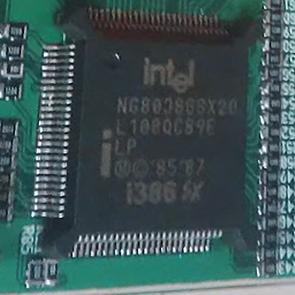
If you want the power of a 386 processor today, you’re in luck: [Pierre Surply] has developed a modern development board for the 80386SX CPU. This board is based on a 386 processor that comes in a LQFP package for “easy” soldering, and an Altera Cyclone IV FPGA.
To allow the CPU to run, the FPGA emulates the chipset you would usually find on a PC motherboard. The FPGA acts as both a bus controller and a memory controller for the CPU. On the board, there’s an SRAM chip and internal memory on the FPGA, which can be accessed through the 386’s bus access protocol.
The FPGA also provides debugging features. A supervisor application running on the FPGA gives debugging functionality via a FTDI USB to UART chip. This lets you control operation of the CPU from a PC for debugging purposes. The FPGA’s memory can be programmed through a JTAG interface.
The project is very well documented, and is a great read if you’re wondering how your old 386 actually worked. It can even be hand soldered, so the adventurous can grab the design files and give it a go. The francophones reading can also watch the talk in the video below.


How about soft core 386 in the same FPGA?
Why?
An real CPU will outperform a softcore in terms of power and speed.
Maybe not. The i386 is produced in a much older, much slower process than modern FPGAs.
I think you need to do a little research. FPGAs can run 32 bit cores at 100+MHz and on a few watts these days. Not great compared to a modern hard CPU (which is why they are moving to combining ARM CPUs and FPGAs on one chip) but plenty fast compared to that generation of hardware. The top end 386SX could manage 40MHz.
It never crossed my mind that this was a slow 20 to 40 Mhz CPU but it is.
I just thought that it was a 386 using a modern process.
Maybe the FPGA would need to be a bit bigger, to fit a CPU plus all the gubbins? x86 CPUs are fairly complex.
That said, I’m sure it’s possible. A 486 might be better, got more done per clock cycle, I think it was the first x86 with a primitive pipeline. Use the SRAM, or a block RAM on board the FPGA, to work as cache, 486s had some on-board.
If it’s possible, you’d have a full PC on an FPGA, that has to be useful for a lot of people. Especially since you could modify and customise the peripherals, or even add instructions to the 486 itself. The downside might be that it’s an obsolete, CISC architecture
Nice and all. But why on earth would you need that and how does “the power of a 386” compare to that of an embedded ARM SoC, say the Cortex-M3 on an Arduino Due?!
Nostalgic reasons, perhaps?
Pretty low, but there is a lot of older industrial DOS stuff that is out there if you are into SCADA. the 386 was and is still used heavily in industrial control stuff. Also a lot of the scientific world runs on them and other X86 PC104 boards so it’s still a viable processor. you dont always need more power.
That was a bit of a joke. The main reason I can think of is tinkering with x86 assembly, or educational purposes.
Radiation hardened applications maybe? It is difficult to make small transistors radhard.
Where does one obtain a 386 “new” processor these days?
I have several from the old days as well as our family’s first Overdrive (ooh aaah) processor. I remember thinking you could run a banana republic on that thing back in the day. DX2? DX4? nah bro, overdrive lol. Our first “pentium” was some Cyrix knock off that sucked rear end and constantly fuddled instructions. They are out there. You will most likely want to look at computer surplus sites online. And of course that guy at the flea market with all of the old machines with the double digit MHz display and ‘Turbo’ button will have a couple of use around :) Best of luck.
Digikey sells ’em
Am I missing something. 5V (386) – 3.3V (FPGA) = 1700 mV / 120 ohm series termination = 14mA. Max clamp diode current is 10 mA from the Cyclone IV DS. Shouldn’t the series termination on the data lines be larger?
It’s series termination to damp out the traces, the IIRC the Cyclone has 5V tolerant inputs so there’s no static power loss, just 1/2*C*V^2 every switching event (where C is the input capacitance plus trace capacitance).
I really, really do not think that Cyclone-IVs are in any way 5V tolerant.
To get I/Os that you can easily interface as 5V inputs you need to step back to the Cyclone-II age.
I understand adding series termination to dampen reflections. But in the explanation from the authors site, it’s stated the 120 ohm resistors are to limit the current through the camp diodes. The data sheet calls out a max clamp current of 10 mA. From my ohms law math, there is 14mA running through them when the 386 is driving 5V output on the data bus. So over time the clamp diodes will degrade. Probably not an issue for this application. Just pointing it out to be thorough.
The Cyclone IV does NOT have 5V inputs. It has clamping diodes. There is a big difference. The diodes will shunt excess voltage to the VIO rail (3.3V) so they must be externally current limited. There will be a drop through the diode so the resulting current might be within spec at 120 ohms. But the board likely will tolerate a bit more (150 to 200 ohms) without retarding the slew rates of the data too much at 386 speeds.
The 80386SX low power model has a 2.4v output high voltage at a 1ma load. The 386 can’t drive 14ma on the outputs, so the 120 ohm resistors are sufficient to place a load on the 386 output transistors to cause the voltage to safely drop below the Altera threshold.
I don’t think you are. The older Cyclones (before the Cyclone-IIIs) had a clamp diode capable of taking 25 mA, but the Cyclone-III and newer devices are 10 mA max.
With newer FPGAs, I really wouldn’t recommend a simple series resistor as a limiter in any case. They usually have pretty tight overshoot requirements (like, 3.6V) that make it really hard for a simple series resistor to stay within spec without gross overkill.
You are assuming that the drivers have 0 ohms impedance and will output 5V.
And you are underestimating drive strength of 1990’s process ICs. :) I’ve built a similar board with a 386SX, a Lattice MachXO2 and SDRAM. And I’ve built an S100 memory board for a 386DX to carry 4GB RAM using a Lattice XP2. It wasn’t as simple as it first appeared. I had a lot of signal integrity problems even using quick switches. I had to eventually go to dual rail VIO buffers and I am still getting conducted noise into the 3.3V supply with a multi-order filter.
Without an IBIS model, I can’t say how much… It is the PMOS driver driving logic ‘1’, so it should be quite a bit weaker than the NMOS.
datasheet shows VOH (min)
IOH = -1mA: A23–A1,D15–D0 2.4 V
IOH = -0.2 mA: A23–A1,D15–D0 VCC-0.5 V
IOH = -0.9 mA: BHEÝ,BLEÝ,W/RÝ, 2.4 V
IOH = -0.18 mA: BHEÝ,BLEÝ,W/RÝ, VCC-0.5 V
Unless they are an order of magnitude more conservative than the typical expected values, I would not say they are that strong. I would expect at least 30 ohms or higher. This is not like those brute force 48mA or even 64mA driver for driver.
Also note that some of the signals (data/address) are specified with TTL type of thresholds and control signal has CMOS ones. I don’t know if they use something similar to HCT for the TTL ones which doesn’t go all the way to 5V.
One thing about clamping signals to rails is that there needs to be something there to sink the current for spikes (AC e.g. caps) or if all the inputs turns high at the same time (DC loads). We had to replace some of the decoupling caps with resistor on Virtex (2?) board because of the FPGA rail (with no other loads) was supplied from a LDO.
The page mentions: “It provides compatibility with 5V devices by enabling a clamping diode which can supports 25mA. This explains the use of 120 Ohms resistors between CPU 5V signals and FPGA IO.”
Yeah, and that’s wrong. That’s for Cyclone-IIs and earlier, not the Cyclone-IV that was used.
Cough. The clamping diodes themselves also have some drop over them, so it’s not a 1.7V drop on that resistor, more like 1-1.1V. I’m actually fairly surprised nobody has pointed that out so far.
So the actual expected current should be a tad less than 14mA, about 7-10mA. Sounds kinda in spec to me, but a larger series resistor might be a bit nicer indeed.
Great idea! I’ve recently been toying with the idea of messing with 486s as that was my first pc. Love the idea of using a FPGA to do all the motherboard tasks.. Hmmmm….
And why do it? Why does anyone do anything retro? You could argue why mess with Amigas/Commodores/Spectrums etc etc..
Turbo button, oh how i miss u so.
Great project! I probably would have put an ISA card edge connector on the PCB to make it more useful but I understand that’s not what this project was about.
Computers seem to get slower as they get faster. The OS and added bloat seems to come faster than advamcements in hardware. I would like to see someone(or personally be able to pick up from windows 3.1 and modernize it without slowing it down. I have a windows 95 and 98 laptop ( both currently broken because lcd inverter voltage went through my screwdriver, early days of learning to service laptops) windows 98 was fast, at first, but upon installing all the recommended updates, it slowed to a crawl. Planned obsolescence, i tell you.
So, does this thing have the RAM on-board, or do i need vintage RAM as well as a vontage cpu?
the main problem of getting old is false memories.
My modern computers with tons of RAM and SSDs run circles around the ones from the good ol’ days… and that is running bloated desktop managers (like KDE) vs. something light, like I was back in the day.
Not sure if this applies to Windows or not, I have not used it seriously since Win 98 days…
I remember back in about 2000 or 2001 I was tasked with installing Windows 3.1 on a K6-III for someone whose wife wasn’t interested in learning the Windows95/98 interface. (Yeah, I know, could have installed 98 and made Progman the shell but they didn’t want that).
Anyway, that K6-III may be ancient by todays standards but it was lightning compared to the hardware most people used to actually run Win 3.1 on. Yes.. it was FAST! Not terribly useful when you want to be able to read modern websites and documents.. but FAST!
A x86 processor emulated in FPGA! No more proprietary IBM code with possible backdoors and crippled encryption..
x86 byte code and CPUs are interesting to explore, my Siemens Sirotec RCM3 that drives my Manutec R15 is 100%
It consists of multiple x86 distributed processing units (Master, Slave, Servo CPUs)
SAB 8086 (a Siemens manufactured 8086), NEC v20 (8088 with higher specs for fault tollerance)
Somewhere I also must have seen an i8086 there.
and the a cool 80186 on every Servo CPU driving two axis.
but the best thing is everything is 74LSXXX LSTTL + some RAM + some UV-ROM + some Hardwirerom + intel extension units PIO, Timer controller etc..
Taking a look at a circuit board is like reading what it does and how it does it!
I love LSTTL
Nice to see someone’s gone and done this. I’ve started, and initially I was thinking I’d do it all with scavenged parts.
I used a heatgun to grab a NG80386SX-20 (not the LP version) off an old motherboard that was badly corroded by a CMOS battery in one corner (not the corner with the 386) and so far I’ve amassed some ICs that could make a hypothetical board.
Interfacing RAM to CPU is the bit I’ve been doing lots of pondering about: I could do it in logic gates, but it will require quite a few. One of the motherboards has some GALs and CPLDs made by Lattice; not sure how to reconfigure those (or if they can be reconfigured).
So a better plan might be to learn some FPGA programming with an iCE40 breakout board. This will mean converting the 5V logic of the 386 to 3.3V, but there are ICs for doing precisely this task, so not a big deal.
Could an ARM do it faster? Absolutely! However, not many ARM CPUs have external interface buses like the 386 has, and many comparative ones cannot interface to external RAM easily. The aim of this project will be to learn about how to construct a computer from bare components, learn about the interfacing and then to see what can be done at the end.
I’ve got a closet full of old 286 and 386 motherboards and CPUs that my dad saved from neighbors starting to sell them with the HD still in them (and all their banking and notes etc). Something like this seems like a great use for a 286 and 386, to teach the difference in how OSes had to deal with the protected modes that came available.
Sure, you could put a softcore 286 in an FPGA, but that’s not always the point.
Now I really want to dig my half-functional PintOS extensions out of notes and go through the dragon book again with a toy like this.
A 386SX? Ugh! The 386SX is a 32 bit CPU on a 16 bit bus. It was developed so chipset manufacturers could use up stocks of 16 bit parts made for 286 boards and continue to produce those old parts to make bargain basement priced PCs. (Note that the price of a low end 90’s PC would buy a mid-high gaming rig today.)
Some companies also got the bright idea to package 386SX CPUs onto adapters to plug in place of 286 CPUs for upgrades. Texas Instruments even managed to shoehorn their 486SX clone into a PLCC drop in replacement for a 286. A 486 minus the FPU *and* connected to a 16 bit bus = ewww, but hey, 486, and the olde 286 could at least crawl Windows For Workgroups 3.11. IIRC it was sold as the “Make-It! 486”. A friend popped one into an old IBM PS/2 286 server, didn’t make much speed difference.
The fastest 386 CPU was the 386DX-40, running without multiplier on a 40Mhz bus. Paired with the 387DX-40 it could outperform a 486DX2-50 with its 25Mhz bus.
One company made a 486DX2-80 plug in upgrade for 386DX-40 boards. It was ridiculously expensive, not much less than a new 486 board and CPU with some 72pin SIMMs. I don’t recall if it used an Intel CPU or the AMD 5×86 chip that was pin compatible with the 486DX. What possibly spurred boosting the 386 to 40Mhz was the Macintosh IIFX with its all 40Mhz design running a 68030.
Speaking of that AMD CPU, did any of you “hotwire” it to force it to 4x speed on a 40Mhz bus? I did, every one of them I had. I had one Micron motherboard capable of 50Mhz bus and the AMD CPU would run beautifully at 200 Mhz, until the external L2 cache SRAM errored. It would work with the L2 disabled but then was terribly slow. I never could find some faster SRAM chips capable of handling 50Mhz so I had to back down to 40Mhz to run the CPU at 160Mhz. Another one I just plugged directly in place of a 486SX on an old board that only did 5V. The ADW version was perfectly happy with 5V and ran cooler than the PQFP on a PCB 486SX-33 it replaced. Win95a on it was very speedy. :)
In contrast, the Cyrix 5×86 486 replacement ran (literally) blisteringly hot. I once barely brushed the heatsink on one and it burnt a blister on a finger. Despite the benchmarks and other performance claims, in real world use I found the AMD to be the better performer, plus the benefits of being cooler – even the hotter running ADZ version was far cooler than the Cyrix.
The FPGA probably has enough Block RAM that you wouldn’t need to add additional RAM into the system. Just emulate it. Which reading it again looks like what he did.
OK, I don’t get this at *all*
A board with a CPU and FPGA – sounds great but the only other things it has are a USB(URAT) and JTAG connector! And did I see a serial ROM to config the FPGA.
Is this some sort of joke. What could you do with a board that has NO (zero zip null) connectors except the programming connectors!!!
And the SRAM, where is that? is it in the underside of the board?
And what about the CPU – Is it in production or do you have to buy one from a 80 old man in some forgotten village in Russia who’s only accepted currency is vodka?
Quote: “Of course, this chip is today considered obsolete but is still the only 32-bit x86 CPU which is simple enough to be integrated in an amateur board”
maybe you can ask hackaday for a subscription refund?
still in production? but he(we) would not BUY it new anyways when we can get them for free (as it is obsolete) you really don’t need to go around asking old people, plenty of young people sell 386’s at your local e-waste recycling collection center, or can “hook you up” with more then you can haul away (minimum quantity) and the prices are…. well… it’s scrap… so maybe 2$ per pound/kilogram ? thats a whole car load full for 15 bucks!
lack of ports? its a proof-of-concept dude, the next version will cover that, why don’t you make a reccomendation.
why are some people always so damm mad when they see someone build a prototype of an outdated system and offer up all the information for free? are they insulted? why?
we do this specifically to get you mad dude, we wasted hours and hours… lol
we will NOT appologise, and we will keep doing it FOREVER!
lol No one is mad here unless you are. These were questions and thank you for your answers.
As for suggestions – VGA, keyboard and mouse ports, SD card for FAT then the rest can be I/O perhaps some 5 volt level shifted on standard 0.1″ pins.
This could tempt me to play with x86. It’s one that I missed.
OK, I see it’s 0.5mm for the FPGA and it looks like 0.8mm for the CPU (Even better!).
I’m a bit worried about the single via used from the Reg to the power plane. Will it work with a ‘normal’ CPU as opposed to the ‘low power’ version you are using? These old CPU’s chewed power (from memory).
PS: As for obtaining one of the 0.5mm pin spaced 80386sx – the options you present are not available here. Can this be bought somewhere hopefully not in the US.
AMD Geode instead (does it still exist?)
Where are the Arduino headers? Can you program it with the Arduino interface?
* – ducks -*
If anyone is looking for the design files, the link no longer works.
The design files have been moved to Github
https://github.com/psurply/lse-pc
Cheers
Updated, thanks.