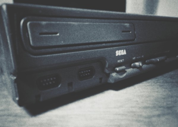
During the 80s and 90s it seemed like Japan got all the good stuff when it came to videogames. In the US there were consoles called the NES, the TurboGrafx-16, and the Genesis. While in Japan they had cooler names like: the Famicom, the PC Engine, and the Mega Drive. The latter was incorporated into a plethora of different form factors, including the little known IBM PC/Mega Drive combo known as the Sega Teradrive. Finding a rare Japanese 1990s PC stateside is a feat in and of itself, and thanks to an electronics hobbyist named [Ronnie] there is at least one Teradrive out there still running strong thanks to an upgraded CPU mod.
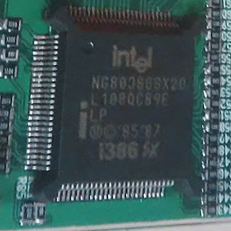
In theory, the Sega Teradrive was a dream-machine; combining the utility of an IBM PC with the fun of a Sega Mega Drive. The dual functionality extended to the video modes where both VGA and composite video were supported. However, the reality was that the final design was less than desirable. The Teradrive shipped in 1991 with an Intel 80286, 16-bit processor which was already two processor generations behind at the time. The meager 10Mhz clock speed was on the lower end of the performance spectrum which meant that many DOS titles ran poorly…or not at all.
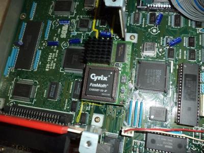
Not satisfied with those specs, [Ronnie] modded his Teradrive with an adapter board containing an Intel 80486 processor clocked at 66Mhz. The upgrade, accompanied with a complete re-cap of the motherboard, brings the IBM PC to 486DX status. This opened up a few new possibilities including the Thundercats Demo in the video below:
Continue reading “Putting The Sega Teradrive Into Overdrive”