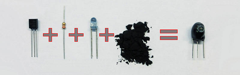
The first integrated circuits weren’t tiny flecks of silicon mounted to metal carriers and embedded in epoxy or ceramic. The first integrated circuits, albeit a looser definition of such, were just a few transistors, resistors, and diodes mashed together in the same package. With this in mind, [Rupert] created his own custom IC. It’s an IR receiver transmitter constructed out of a transistor, resistor, and an LED.
The attentive reader should be asking, “wait, can’t you just buy an IR receiver transmitter?” Yes, yes you can. But that’s not a hack™, and would otherwise be very uninteresting.
[Rupert]’s IC is just three parts, a 2n2222 transistor, a 220Ω resistor and an IR LED. With a good bit of deadbug soldering, these three parts were melded into something that resembled, and had the same pinout of, a Vishay TSOP4838 IR receiver. The epoxy used to encapsulate this integrated circuit is a standard 2-part epoxy and laser printer toner. Once everything is mixed up into a gooey slurry, it’s dripped over the IC producing a blob of an integrated circuit. It’s functionally identical to the standard commercial version, and looks good enough for a really cool project [Rupert]’s been working on.
Thanks [foehammer] for the tip.


That isn’t an integrated circuit in any sense of the word. It is a potted circuit.
The construction technique that is halfway towards a “full” integrated circuit was a thick film or thin film hybrid circuit. And it still is, especially for high frequency analogue/RF circuits.
For examples of hybrids including transformers, have a look at some pictures from a late 70s Burr-Brown calendar, at https://entertaininghacks.wordpress.com/2015/07/07/images-of-late-70s-burr-brown-thick-film-hybrid-ics/
Thanks for the link. Amazing pictures – those devices must have cost a fortune.
Everything cost a fortune back then!
Well, making something like this today would still cost a fortune.
For a modern thick film hybrid, see http://www.eevblog.com/forum/testgear/ininiimax-7ghz-active-differential-probe-teardown/msg736858/#msg736858
Probe cost at Newark/E14: $7300
Bottom Right – PSoC without the ‘P’
I remember seeing one of those in an antique “X-in-1” electronics kit. It was labeled an “integrated circuit”, and had a clear cover so you could see the tiny components inside. I saw it after real silicon die ICs were common, but before SMD, so I was amazed at the miniaturization of discrete components.
Now pretty much every circuit board looks like what they used to call an integrated circuit.
“The first integrated circuits, albeit a looser definition of such, were just a few transistors, resistors, and diodes mashed together in the same package.”
The author is very clear, and you didn’t bother to read the article.
I did read the article, did understand what the author said. The author has used a definition that was, charitably, transitory and became obsolete half a century ago. Jack Kirby didn’t become famous for (re)inventing potted circuits!
For the avoidance of doubt, the normal modern definition of integrated circuit is everything on one piece of semiconductor material. If you don’t use that definition, then you might as well claim that discrete component soldered onto a PCB is “a looser definition” of an integrated circuit!
Lots of components soldered together and encased in epoxy equals “potted”. See, for example, https://en.wikipedia.org/wiki/Potting_%28electronics%29
>The first integrated circuits, albeit a looser definition of such, were just a few transistors, resistors, and diodes mashed together in the same package.
Brain, I think you are mixing up “Integrated Circuit” and “Hybrid Circuit”.
https://en.wikipedia.org/wiki/Hybrid_integrated_circuit
The term integrated circuit has been reserved for monolitic circuits since the beginning. The glob described in the article is not an IC. It also isn’t really a hybrid circuit. Its three components embedded in epoxy.
Listen YOU !!! Quit questioning Brian! He’s an expert!
Hey Brian,
Thanks for the cool new technology. Do you have a link to the kickstarter so I can contribute?
Thanks!
You should go back to facebook and stay there.
what does facebook have to do with anything?
I’m assuming you have some ‘followers’ who will approve of your bullshit. And I’m suggesting you should be happy with those people who try to amuse you, and not bother the larger world with your type of ‘clever comment’.
Also, one comment regarding the “IR-Receiver”: You can actually buy such a device in integrated form – it’s called a phototransistor and contains a photodiode and transistor on a single die. No need to build it from discrete components, you will only add parasitics.
That said, the TSOP 4838, which is referenced in the article, is actually a full photoIC. It has also contains a demodulator for the 38kHz IR carrier…
Just one quibble, a phototransistor doesn’t contain a separate photodiode. It’s just a transistor, exposed to light. In the old days, when transistors came mounted in metal cans, sometimes a hacker would cut the can open to produce a phototransistor. I think most transistors would respond to light, given a chance. I suppose phototransistors use ones specifically designed to be light-sensitive to a particular degree, but the effect works on all semiconductors.
I don’t see why he’s bothered doing this particular thing. It doesn’t demodulate the carrier, doesn’t have the smart gain-control. He’s essentially built a phototransistor instead of just buying one, for some reason.
>Just one quibble, a phototransistor doesn’t contain a separate photodiode. It’s just a transistor, exposed to light.
It’s true that normal bipolar small-signal transistors are also photosensitive, but that does not mean they are optimized for that purpose. Phototransistors usually have an increased base area and and base width to form the photodiode part. Doing this to a normal transistor would make them much slower due to higher junction and diffusion capacitance of the base.
Yeah I did mention that phototransistors are specially designed for the purpose.
To make an even smaller and more specific point, it’s not just small signal ones, I’d bet any old bipolar transistor would be photosensitive too. As you mention, base size would be a factor in sensitivity.
I wonder if it’d work on FETs too? Is the photoelectric effect in question essentially a tiny solar-panel creating enough voltage to activate the base? So the transistor is switching in the normal way, dependent on the base, but in this case without an externally applied voltage.
Or do the incoming photons free enough electrons in the bulk matrix to allow it to conduct? After all that’s how a photodiode works, where the reverse-biased breakdown voltage falls to almost zero, upon exposure to light.
I don’t need equations. I certainly don’t WANT equations! But a nice explanation would be useful.
EPROMs will work as very low output photovoltaic cells. Uncover the window, expose to direct sunlight. Daisy chain a lot of them Vcc+ to ground.
I wonder who else here has scraped the black paint off an OC71 ? :)
Yep, I also did. The red dot showed which pin was the emitter (I think).
That being said, the PN junction of the NPN transistor IS the photodiode. There is no separate diode in the same package. Every (bipolar junction) transistor in the universe IS two diodes, just as every apple in the universe IS a fruit. There’s no separate fruit in the same skin ha ha
And every diode is also photodiode if light can get to the junction.
Only worked until the manufacturer (Mullard?) got wise to the trick and started filling it with opaque epoxy! Which neatly brings us back to the OP’s hack.
Its a IR transmitter not a receiver, and you cant buy them in a T0-92 style.
Just out of interest, have you built a CPU out of a CPLD? Has anyone? Got linkz? Sounds interesting, a few mental exercises in there.
Well, after reading the article I feel like it isn’t receiver part, but transmitter. 2N2222 with 220Ohm base resistor – and the IR LED got no series resistor, meh.
I made such as ICs when I was ten or eleven years old. I soldered astable multivibrator made of two transistors and few passive parts into matchbox and filled empty space with wax. I was very proud of it and definitely would write a blog about it, having the chance.
Go one better, tiny PCB, use surface mount parts and do the same thing. makes a lot cleaner end product and you can get a lot smaller. clever bit on the toner to tint standard epoxy.
great hack… i guess…. really don’t see the point…… seems like one of those “because i can” hack. anyone want to enlighten me as to the practical applications where this would come in handy?
didn’t read the guys OP to see why he did it, but sometimes it is for the challenge of doing something. Sometimes it is because you need a functionality and you don’t have/want to wait for the right part. Sometimes it’s simply that the “right” part doesn’t exist or is expensive. The reason isn’t as important sometimes as the result.
usually with these sorts of things, the reason for building is unknown and the result (practical application) is discourse. i’ve noticed this phenomenon as well with works of art from the last 800 years.
Just to introduce a ray of light into these dark comments above; what I found useful was his method of mixing epoxy and black toner in order to create a black blob.
Also, I agree you can buy things, or make fancier things yourself, but sometimes, for instance on a rainy Sunday when you finally have time to work on that project you’ve been meaning to for weeks, you just don’t have the time to make something fancy or order something and you just want to hack something together. And I think that’s ok.
My first memory with these “(not) integrated circuits” were those ancient discrete RTL boards I bought as a kid in the seventies from surplus stores. They had matrices of logic gates each one built off one oddly relabeled bjt and some resistors and diodes, all sandwiched between the bigger board and much smaller ones, one per gate. Took hours to dismantle, but was well worth the effort to gain a drawer full of useable parts.
What the hell are you naysayers even doing on this site? I’d say you are paid shills, but your attempts are too pathetic even for that.
Similar methods are used when replacing impossible to find direct replacements, such as two value capacitors. You’ll find guys repacking two equivalent modern caps inside the wax cylinder in order to “keep apearances”. You’ll also see it with common circuit configurations. Smoothing caps on IC’s or DIP switches ontop of shift registers for breadboarding. I never choose to pot them though. I don’t care for potted circuits unless unless there’s a damn good reason for it and the function is well documented.
Like a recapping I did on an old ford galaxy am radio a couple of years ago.
Somewhere on HaD is a plug in board made to replace an IC for an HP frequency generator or counter, and another one made to replace an unobtainable voltage reference part in another old piece of test equipment.
If you’re going to be building replacement integrated components using discrete components and/or other ICs that are as subset of the circuit inside another IC, start small by globbing together a functional duplicate of something like this IR part.
Black hot melt glue.
Easier & quicker.
Perfectly durable.
Mike Szczys beat Bryan to this concept of potting a dead bugged circuit before, but it as far more interesting. Although this doesn’t add toner to the acrylic.
http://hackaday.com/2012/04/13/free-formed-circuit-protected-by-a-brick-of-crystal-clear-resin/
the OP posts so many articles theres bound to be a small mistake and im not mad…
but all you readers/commentors (people who have time to analize things) should be ashamed
integrated circuits were invented way before transistors or “monolithic”-anything!
im not just talking about combo-tubes(diode plus pentode), im talking about tubes with resistors and capacitors!!! or WHAT ABOUT TUBE-OPAMP MODULES!
three (miniature) tubes in the space of one, plugging into a socket simillar(or same?) as a tube.
now THATS integration (and fire hazard lol)
So, if you asked me to get you a computer, you would feel I had done what you asked if the computer walked in the door, said 12 times 12 is (a) gross, smiled sweetly and fluttered her eyelashes.
After all, for most of human history “computer” was a job title, usually for women.
The purpose of language is to share understanding and share thoughts (exceptions: politicians and religious demagogues). Calling a potted circuit or opamp module an “integrated circuit” is either misguided, obfuscatory or only of historic interest.
BTW, using correct punctuation and capitalisation would make your posts look more professional.