If you’re a KiCad user, as many of us here at Hackaday are, you’ll be elated to hear that KiCad 4.0 has just been released! If you’re not yet a KiCad user, or if you’ve given it a shot in the past, now’s probably a good time to give it a try. (Or maybe wait until the inevitable 4.0.1 bugfix version comes out.)
If you’ve been using the old “stable” version of KiCad (from May 2013!), you’ve got a lot of catching-up to do.
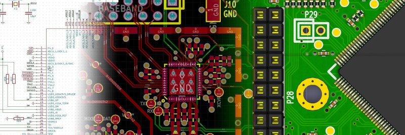
The official part footprint libraries changed their format sometime in 2014, and are all now hosted on GitHub in separate “.pretty” folders for modularity and ease of updating. Unfortunately, this means that you’ll need to be a little careful with your projects until you’ve switched all the parts over. The blow is softened by a “component rescue helper” but you’re still going to need to be careful if you’re still using old schematics with the new version.
The most interesting change, from a basic PCB-layout perspective, is the push-and-shove router. We’re looking for a new demo video online, but this one from earlier this year will have to do for now. We’ve been using various “unstable” builds of KiCad for the last two years just because of this feature, so it’s awesome to see it out in an actual release. The push-and-shove router still has some quirks, and doesn’t have all the functionality of the original routers, though, so we often find ourselves switching back and forth. But when you need the push-and-shove feature, it’s awesome.
If you’re doing a board where timing is critical, KiCad 4.0 has a bunch of differential trace and trace-length tuning options that are something far beyond the last release. The 3D board rendering has also greatly improved.
Indeed, there are so many improvements that have been made over the last two and a half years, that everybody we know has been using the nightly development builds of KiCad instead of the old stable version. If you’ve been doing the same, version 4.0 may not have all that much new for you. But if you’re new to KiCad, now’s a great time to jump in.
We’ve covered KiCad hacks before, and have another article on KiCad add-on utilities in the pipeline as we write this. For beginners, [Chris Gammell]’s tutorial video series is still relevant, and is a must-watch.
Thanks [LC] for the newsworthy tip!


Is the UI still insane, especially the mouse? Maybe I’ll give it another go and see if I can stand it more than 5 minutes this time without wanting to throw my mouse out the window.
/ DipTrace user.
I failed.
If I click and drag on a wire, I WANT TO MOVE THE DAMN WIRE.
If I click and move from a terminal point I want to MAKE A WIRE RELIABLY (sometimes it works, sometimes not, sometimes it draws a wire, sometimes it pulls a select rectangle, sometimes it opens the dialog for the component, ARGH the same action should not do different things depending on the time of day, season of year, or angle of tongue)
If I click and drag on a component, I WANT TO MOVE THE PART.
If I move a part, I DON’T WANT IT TO DISCONNECT FROM EVERYTHING AND HAVE TO MANUALLY RECONNECT IT.
Yep it seems that they have zero clue how to design a UI… I’m sticking with Eagle.
Yeah – having to export the net list, define the part, and then have to deal with crappy ui on the PCB layout. I was hoping to use it, but I might as well shell out the $1600 for the awesome version of Eagle (so I don’t have to worry about size limitations)
That shows how bad it is, as Eagle as an UI is quite “meh”.
KiCad just lacks a general sane user-flow. And the power-user keep defending it.
I dont think they are power users, I think its the same problem Gimp had for all those years – programmers doing UI. They dont use the software, they are just coding it.
There’s nothing wrong with using Eagle if that’s what you’re comfortable with, but in no way is it a UI high ground – it’s got a whole host of it’s own atrocities. I gave up on Eagle after the third time I had to relearn it’s quirks from scratch after not using it for an extended period.
As far as I’ve used, almost every EDA tool has a crap user interface. They seem to be designed in a vacuum stuck in a time machine set to wind back to about 1999. The only ones that seem to come close to getting it right are Altium or maybe Upverter, and I’ve only had the pleasure of limited exposure to both. Everything else is as shit as anything else, including LTSpice, Eagle, KiCad, Orcad and GEDA. Mechanical CAD was the same until solidworks came in and wiped the floor with everyone, let’s see someone make a decent open-source equivalent to that!! (Here’s looking at you FreeCAD, although I haven’t seen you since 0.13. Good luck and get it done!)
At least KiCad works very well once you can get around the rubbish interface, and is free and in very active development.
If you think the user interface is broken, fix it yourself or make clear suggestions to the team that can!
I didn’t think LTSpice was all that bad although it’s irrelevant if you want to make a PCB. As to the others… I think you are giving 1999 a greatly undeserved insult. I think 1989 might be a bit more apropriate of a comparison!
Wow, switching back to Eagle to get a better UI only shows how bad the situation is :) After working with (DOS) OrCAD and Tango, then Protel & Altium I just can’t stand Eagle’s UI. Same about KiCAD. Looking for an affordable alternative I’ve purchased DipTrace, but it has its own quirks and weird behaviours. How come there’s nothing to chose from, really?
It looks like a single click places a wire, while clicking and dragging overrides it to a selection box.
Kinda seems like a bunch of neck-beards decided that convention was stupid and wrong, and must be changed. I.E., it’s marginally more efficient for certain workflows if we force everyone to relearn everything and make to totally un-intuitive. Maybe UI patch or plug in can be made. It’s open source after all.
That’s exactly what’s happening.
http://www.ohwr.org/projects/cern-kicad/wiki/WorkPackages
“Study ergonomics of various commercial/proprietary PCB applications (when in doubt about any particular UI solution, check how it has been done in a certain proprietary app that is very popular among OSHW folks and do exactly opposite).”
EDA software in general has terrible UX. Most FOSS software unfortunately suffers from the same condition. When you combine the both, the outcome is generally not pretty.
There’s definitely a void to fill in this space – you see web front-end developers writing slick and intuitive web app interfaces with the latest whatever.js, but no love for innovative user experience in the desktop application realm. Is the barrier to entry for quickly mocking up and redesigning a UX too high? Are people just not interested enough? Are there too many differing opinions on what’s “right”?
How can the community resolve this problem – does a FOSS-centric UX best practices guide need to be writing and elevated to holy bible status?
That line is pretty clearly a dig at Eagle (“a certain proprietary app… very popular among OSHW folks”). No one thinks Eagle has a good UI — not even Eagle users.
The action item is: “Study ergonomics of various commercial/proprietary PCB applications.” Seems reasonable.
Maybe I should just quite complaining and try and do it myself. The bar is so low that even a bad job will be a huge improvement. It would be quite easy to rip off the best UX ideas from online EDA tools, and even other apps that involve similar interactions. EDA UIs are stuck in the 90s. That’s one thing if it’s a primarily command line based dev environment, but and EDU is a GUI, and it has to be good.
Eagle sucks, horribly, but the opposite of Eagle isn’t necessarily good. Instead of worrying about what everyone else does, they should just try to embrace the much broader evolution of GUIs over the last 20 years.
Imagine if we had an inference engine like SketchUp. We could crank out new footprints in a second.
The infamous *interference* engine in sketch3D that do stupid things. Can’t they at least let me use short cut keys LIKE x, y, z to say which axis I want things to move? I guess I want it to be closer to a CAD more than a drawing program. For doing simple things it is good, but even then some simple operations aren’t intuitive.
The barrier of entry is too high – designers usually aren’t programmers. If kicad (or other software) did their UI in HTML/CSS/js or even just had a skinning DSL that would make a big difference.
It’s really hard to do that though.
I think it fell into the programmer centric way of thinking. Instead of making a program that is user centric i.e. most intuitive way of doing things, they make it easier to program the darn thing. It is harder to make a program around a event driven UI than throw scripts to link batch jobs at a problem.
Hey they aren’t serving the users – they are just scratching an itch and users just happens to be a by product. Thus the whole RTFM or RTF Source code attitude. Don’t blame the mighty programmers. :P
If you use any EDA tool, then the UI of *every other tool* looks insane. But you fail to notice that your chosen tool is also just as ridiculous – it’s just the one you happen to be comfortable with.
If you like Diptrace, then keep using it. If you want to get the benefits of another tool, then you’re doing yourself a disservice by demanding that it behave according to your own unconscious biases. Suck it up and *learn* how to use it, or choose to stick with the tool you know.
Agree. I started with P-CAD, then switched to kicad. Kicad was differently strange to me, but when I spend some time with it and made 2-3 boards I really loved it. Then I tried Eagle. That was really alien technology for me.
The point is though that KiCad (and to be fair, not *just* KiCad, this is a disease rampant in EDA) is not intuitive an intuitive interface, and is not an easily discoverable interface.
Take somebody who has NO preconceptions about how an EDA tool should work but a basic understanding of electronics and a fluency in general computer software and say “copy this simple circuit I have drawn on this bit of paper into KiCad” and I posit that user will be FRUSTRATED BEYOND BELIEF. Put them down in an INTUITIVE tool like DipTrace or even Fritzing and they will have a much easier time to produce the result required.
KiCad’s interface has been developed by the programmers who use it, that is a BAD idea, it has lead to inside knowledge and the opinion “what is so hard, all you have to do is press X-Y-Z while doing A-B-C”, for the programmer they KNOW this, they made it that way and so it has become natural to them, it’s not natural to somebody coming to the software, it’s not intuitive.
I can’t even CTRL-C to copy a component and CTRL-V to paste it. I can’t even select a component and select Edit > Copy. I’m sorry, but if a software can not handle such a fundamentally basic and standard concept of user interaction (seriously, CTRL-C and CTRL-V, copy, paste, COPY AND PASTE) then it’s user interface is wrong. Simply. Wrong.
Well, i did not get “frustrated beyond belief” when i switched from Eagle to kicad. I’m not saying there aren’t any things to improve, but you don’t need to be such a drama queen.
I don’t think all EDA tools are equally insane. I don’t want to advocate any particular product, but e.g. Protel’s user interface was much closer in look and feel to other Windows applications (e.g. shift + click to select, etc.).
KiCAD’s UI is way too strange for regular users. For example – isn’t it surprising, that window selection starts moving selected elements? Or rotates the selection, if Alt is pressed?
You know, there is that thing — keyboard shortcuts. Life gets easier when you use it (although kicad doesn’t allow you to reconfigure then, damn). Expecting kicad would work point to point as *your favourite cad* is strange, isn’t it? But you are right, kicad is far from ideal, there’re a lot of thing to improve.
You have to press “G” to grab a wire and drag it around.
Once you get used to the keyboard shortcuts, I found KiCad very fast to work with
I found it frustrating too. I know it all makes sense to someone but I think it’s not very intuitive. Design tools need to be intuitive. People who design things don’t the tool getting in the way.
Most OSS software is written by programmers who think everyone else is a programmer. Making a software useable to people who don’t give a rat’s ass of the software internal working but need it to be easy to understand and operate requires someone else who kicks the programmers in the butt and *forces* them to think about usability. This requires culture, people, time and money -ie, a company- and is the reason why a lot of great OSS projects on paper (not all, luckily) fail miserably for being masterpieces of code that nobody among those who need them most would want to use.
Are repositories going to be getting this updated KiCad? I’m using Mint and the latest version shown is 0.20131208+bzr4024-1ubuntu2
I’m also curious to know if the draw speed is improved in pcbNew? It’s a bit chuggy on my system while zooming in and out.
Give OpenGL mode a try. Its a lot faster, however it is missing some options that are in the default view (somehow this is a thing.).
Not only faster, buy nicer. It makes the program look like something from the last few years, else it just looks like it was made in the 90s. Not that it matters, but it helps.
It’s a “thing” since the code base is not ready yet to integrate all the functionality to the one mode. People should follow their developer mailing list more often and read the forums…
Or they could be more vocal about the state of the program and why it’s like it is and what they’re going to do about it.
That depends on the repository maintainer.
I installed RC2 recently, just by following the easy steps on the kicad website http://kicad-pcb.org/download/linux-mint/
It seems that the PPA is still at the RC2 atm, or the documentation hasn’t been updated yet. But in any case, it was installed in no time.
About all the comments regarding the user interface, I agree it can be improved, but I also think it is much less dramatic than what you might expect from what people say. I use it very irregularly, and when I get back to it, it takes some time to relearn some things, but it never takes long and once you get going, I feel like I can do things very quickly, except when you’re doing microwave stuff. Bends, mitered corners and all those things that are important when dealing with high frequencies, are lacking. I’m quite optimistic though, at the rate this software is improving it has a bright future.
Is this version with the old problem to connect libraries? No, thanks. I cant believe that someone can use this. It’s insane.
I don’t know. How about you try a little harder to explain what the “old problem to connect libraries” actually is.
No Windows build? All I see on the download page is a link to RC2
I quit kicad 1 year ago after so many bugs.. Still thinking if this new release is finally good enough..
People use auto-routers?
I do, although all the PCB’s that I’ve done so far haven’t involved any really high speed signals (20 MHz at most.)
Semi-auto? hell yeah. Push and shove and auto hugging is amazingly helpful.
Yeah, I agree. To be honest I’m fairly amazed anyone would consider a push-and-shove router an “auto-router.” To me, that’s just… a router. Without it it’s just a layout editor that can draw lines.
For routing an entire board? Probably not. For selective auto-routing of tedious and non-critical board regions? I would be more inclined to say yes..
Who could resist intuitive UI of Gimp??
I’ve been using KiCad for my personal projects for the last couple of years, it has some quirks, but I actually think I like the workflow much better than Eagle (which I’ve used for a few boards). I’ve been getting to grips with PADS at work, if you think KiCad has a funny UI you should try that!
I’m very excited to try out the new push and shove router.
Well, I’d love to download the stable 4.0.0 version, but all I can find on download page is 4.0.0 RC2 http://kicad-pcb.org/download/windows/
Or the RC version is actually stable version? Should I look in “recent builds”?
There is the “almost there”-release (no kidding, it’s named like that), but maybe it’s better to wait a little for the actual, real release. It’ll probably be there today or atleast within couple of days.
This was a reply to jaromirs and others wondering.
is it about time to update CAELinux? (last modified 2014-03-09)
Does this program suite’s parts library still not link Part name/number -> Schematic symbol -> pcb footprint -> spice model?
Without that all you do is guarantee footprint errors.
cmon, whats additional 30 clicks per part among friends?
Yay, click-fest!
Letting a layout (non-EE) team in a large project to pick chip packaging is asking for trouble. The design authority should remain with the EE team that design the circuit. There are so many things such as adding the right amount of decoupling caps for each power/ground connections, thermal consideration, chip pin spacing vs safety etc global concerns that you can’t expect someone else to randomly pick a footprint to suite the layout.
One logical solution to the UI/UX problem is to decouple it from the rest of the program. It’s essentially a specialized kind of CAD program API that can be called from a separate interface program (preferably user definable, and preferably compatible with multiple CAD programs.) This kind of separation will also allow hardware to act as part of the UI/UX (akin to programmable keyboard, space pilot, gamming keyboard, etc.)
Oh Gawd – That’s the whole “Convergence” mistake thinking again! This is a single-purpose application and it should focus like a laserbeam on that specific purpose.
KiCad and the CERN-involvement is a miracle to me.
Instead of doing the obvious they start working on the internals. The obvious you may ask? Simple: First create a slick, simple, consistent, fresh user interface. Something that attracts new users and helps them to grow with their needs and to learn how KiCad works. Old users? Sorry, you have to learn new.
Second: create very very very easy part and footprint maker (since I’m still in love with diptrace: they do it right!).
Third: build some online parts database. Search a part? It’s already online. If not, make it, put it online, earn your fame! Second and third aren’t really two steps, they go hand in hand and would create a really great product. Make it fast and simple and you rule the world. (Again, my current love diptrace did it all wrong: parts publishing is slow, cumbersome, annoying…)
Fourth: add a consistent, understandable project management system guiding from schematic to pcb. Let if follow the production process with simple assistants.
Fifth: add fresh ideas. I would love to have a scratch book and to-do-list linked to parts and groups. Adding things I have to think about, to change, to do, links to online resources. BOM? Why don’t you add a simple spread sheet?
And please, I don’t want different applications with save, import changes, update etc… (diptrace did it right: very easy to update schematic to pcb) Follow the production process: if it isn’t produced, apply changes. If it is produced, create a branch.
With KiCad they have a great backend technology what waits for some inspiring user experience. I wish they put more resources in global project strategies and UI development.
(Copy of my review from elsewhere… and by the way: I still thing diptrace is a dead horse. Still looks nice but starts to smell.)
KiCAD is not the Arduino of EDA tools. It is likely that those at CERN supporting KiCAD actually invested the time to learn how to use it first, and while they may want to make the UI easier for beginners at some point, they probably decided there are more important things that need to be done first.
Once I had seen the famous KiCad push-and-shove demo I seriously considered finally ditching Eagle. I don’t understand how Eagle still lacks any manual routing assistance (ever tried moving a bunch of curvy, parallel traces? I must have wasted a week of my lifetime doing that). The command line interface is handy for the dev-team only, and oh how I miss moving the components/traces step-by-step with arrow keys instead of aiming with a mouse.. Also 3D view is absent, while several useful 3D Gerber viewers have been coded by just a single, devoted hobbyist (..so it can be done). Then there’s optimization.. or lack thereof. Adding a part means waiting for DB indexing, which of course uses just a single core out of 8, and zooming in/out fluently requires a Crysis-capable CPU (for more complex boards) as GPU-based acceleration is non-existent. How do they even charge for another release? Having seen it in use, my GF called Eagle “an advanced MS Paint” and there is a point about it..
So I instantly downloaded KiCad and discovered that you can not edit a schematic while watching things change in PCB window. I got so used to it I thought it was a standard feature, but it didn’t turn out so (it really helps while swapping gates / GPIOs around). Eagle’s library-based device-symbol-layout scheme, while a bit redundant, is a ton more intuitive than separating schematic and PCB design entirely.
All of that left me frustrated and still using Eagle.. :(
On large EDA schematic and layout are separate programs (and good auto routers are licensed separately). At work typically there are teams of layout people working with the EE doing schematic in parallel and there are special way to sync up the design in a work flow. Eagle’s scheme is more suited for hobbyist or tiny one man operation/consultant. Each has it own market.
I use curvy traces only when I need it around mounting hole etc when space is tight or doing turns on flex circuits. The 45 degrees turns are the easies, boring standards that everyone uses. (Yes we even use that at 3+Gbps signalling.) They are pretty easy to move as a group. Having some manual assist would be nice.
Thanks, I really appreciate the answer. The largest EDA team-op I was involved in required three people taking turns, so I was unaware of heavy duty software trends. I can still see some benefits of Eagle scheme, however.
Regarding curvy traces – what I meant were bunches of parallel traces, cascading trough straight and 45 degrees.
I wish Eagle would not let you route a trace any closer to another trace/pad than specified design rules would allow (ideally highlighting the trace once the limit is reached). Seems relatively simple to implement – the functions are already written for DRC verification. If only the code was open (sigh) I’d happily dig and dig around to add it. The way I do it now involves flooding the board with GND polygon and sticking to its border while routing around the obstacles.
I cheated a bit by drawing a trace or a donut that is x mils thick. Place the donut over a via and that shows me exactly where the minimum clearance is. The thick trace shows me how close I can pack traces and can be a useful indicator when put them on the edge of your traces and move as a block. Having the layout tool showing me where the DRC boundary would be very nice.
The flooding with GND trick also works, but I learn to ease back a bit on plane fills as they affect yields and create shorts when using cheap PCB fab houses.
To all the folks complaining about the UI you’re right. It does suck, no it’s not like your favourite EDA, yes you need to learn hotkeys.
I don’t have any solution to the UI problem other than if you have a better idea write a patch or even a mockup of improvements. UI stuff is huge problem with a big chunk of opensource software which really sucks because a lot of it is extremely powerful. Developers need to make it easy for designers to contribute their skills (abstracting the UI from the backend code – easier said than done of course)
Since we are bitching though….
My major gripe with Kicad is the lack of scriptability. One really nice thing with GEDA was you could automate a lot of stuff with scripts and Makefiles. There doesn’t appear to be any way with the python scripting to say automate exporting the gerberfiles, or generating some SVG’s of the schematic (that would be a nice git commit hook).
My other complaint is the library system…. what a total mess. Soooo confusing.
When I started learning KiCad, I used Ashly Mills video series which is great https://www.youtube.com/playlist?list=PLCNJWVn9MJuORLQ3ds_U3D7RILfE4zdoL
I cant believe nobody has listed Pulsonix. While not hobby priced it is by far my favorite EDA tool. Having reliable spice simulation on the schematic layer is a huge boon and the PCB tools are top notch.
As for a more affordable there is NI Multisim & Ultiboard. A more clunky interface but VERY approachable and everything in one package.
In this version, is making an hatched ground option provided? It is very much required when we are making capacitive touch switch on PCB.
It’s interesting to me to look at this discussion from another perspective. I learned on Eagle, and even used it for the first few projects I did working as an electrical engineer. But we switched over to PADS by MentorGraphics (which, as I understand it, is one of the top EDA packages on the market, with Altium seeming to be it’s main competitor). I’ve since done several hundred designs in it and am (now, finally) quite comfortable using it. For reference, the basic license of PADS that I use cost $7000. Altium I think is about $8000. We’ve since hired another engineer that uses Altium for his personal projects so I have a little insight into it as well.
A few thoughts: Poor interfaces are not limited to the less expensive / Open Source EDA world. PADS’ interface is archaic. It was clearly designed to run in 16 colors, each time you move, scroll, zoom, it visibly redraws the screen (on a nice i7), there is a completely different procedure for making an arc when you are laying a trace than there is if you are making a silkscreen arc. DFX files come in as hundreds of disjointed segments that aren’t even touching if you zoom in, and you can’t fix them, you have to trace over them! The only way I’ve found to get images in (for logos, etc.) is a 3D party 16-bit DOS app!
But! It has online/real time design rule check (DRC) / enforcement. And it has a (basic) push and shove router. Those things alone as so incredibly valuable that I will never again consider an EDA package that lacks them. Routing a dense board with Eagle is a painful process of setting grids, running DRC, fixing errors etc. and you’ll never get it as tight or clean as you can with online DRC. PADS just keeps the traces the right distance apart. There are boards I did with very little trouble that would have been a nightmare in Eagle. It looks like KiCad’s push and shove is better than PADS.
I also use SolidWorks for our mechanical designs. Great stuff when you get used to it. Man I wish they’d use their interface smarts to write an EDA package!
I’m very, very excited to see where KiCad is going. I can see it overtaking the professional packages before long.
TL;DR: Online DRC and push and shove routers are worth their weight in gold! Poor interfaces are the norm (and you can get used to them)
Word.
When I started learning KiCad, I thought the design-rules enforcement thing was silly, but now I absolutely love it. Coupled with push-and-shove, you’ll never need to autoroute anything. When you lay a trace down, it’s legit. And when you need it to move, you don’t have to rip it back up, just nudge it.
Contrast with Eagle, which I used for ten years or so. I developed this pseudo-push-shove method where I’d rip up a couple wires, auto-route them, rip up some more, auto-route, etc. Then run the DRC and repeat for any offenders. It actually worked ok, but in retrospect it was a bit of a hack.
On the UI: Zooming in KiCad with the scroll wheel is non-standard, but in my opinion it’s an improvement once you get used to it. Other things, like mode-dependent menus, still trip me up even after nearly two years of practice. Sigh.
Great! Now we just need to get part manufacturers to distribute digital versions of the footprint drawings that are in their datasheets, in some universal high level language format. Or just encode the data into a QR code or something, right on the datasheet page, or as a copy-and-paste code page, so all the info comes along with the datasheet.
Bringing up new parts in CAD packages is always one of the hardest parts, especially when using tools like EAGLE.
Surely such a format must already exist? PADS or OrCAD or something like that?
Also, why isn’t there an Eagle Library manager application? It’s just a bunch of XML parsing …
And how about a plugin that can connect to SnapEDA and auto-pull footprints, symbols, etc?
I’m finding myself returning to KiCAD after realizing what a disaster diptrace is and how buggy it is. KiCAD is certainly not perfect but I am finding it faster to use than diptrace with the keyboard shortcuts, you have to know the shortcuts or use the right click menu options where you find many things you think KiCAD didn’t have. Diptrace has not made any real progress in over a year and i have gotten pathetic excuses from them. so I’m back on Kicad and at least for loom diagrams it’s great.
I want to creat a arc trace? How do?