I like to think that there are four different ways people use FPGAs:
- Use the FPGA as a CPU which allows you to add predefined I/O blocks
- Build custom peripherals for an external CPU from predefined I/O blocks
- Build custom logic circuitry from scratch
- Projects that don’t need an FPGA, but help you learn
I’d bet the majority of FPGA use falls into categories one and two. Some FPGAs even have CPUs already built-in. Even without an onboard CPU, you can usually put a CPU “core” (think reusable library) into the chip. Either way, you can always add other cores to create UARTs, USB, Ethernet, PWM, or whatever other I/O you happen to need. You either connect them to a CPU on the chip, or an external one. With today’s tools, you often pick what you want from a list and then your entire project becomes a software development effort.
The third style is doing full up logic design. You might use some cores, but you don’t have a CPU involved at all. You configure the FPGA to execute precisely the logic functions you need. Of course, if you are creating a custom CPU, you will sort of blend all of these styles together at different points in development. Other developers may build systems that include a CPU on the FPGA, some custom cores, and some full-blown logic development, so the lines can and do blur.
I’ll ignore the fourth style. It is great practice to do a traffic light state machine or an LED flasher in an FPGA. Practically, though, you could just as well use an Arduino or some other microcontroller to do that.
Why Use FPGAs?
With the first two styles, the reason for using an FPGA is clear: those developers just want to mix and match prebuilt cores. Just like building things out of Lego bricks, it might not result in an optimal structure, but you can get a lot done with little effort. The downsides are mostly cost and often power consumption, depending on the device.
The reasons you use an FPGA to do “pure” logic design are the same reasons you develop using discrete logic in the first place. FPGAs can implement very high-speed logic. Where a CPU has to execute a bunch of instructions to do things, the FPGA just has dedicated logic to do whatever you need, often in one clock cycle.
Also, most operations on FPGAs run in parallel. Say you build a PWM block and put it on the FPGA (something we’ll do below). If you decide you need two PWM blocks, they will still operate at the same speed. If you need 20 PWM blocks, they will also run at the same rate as a single block.
An FPGA’s ability to run at high speed and in parallel makes it an excellent choice for parallel processing and high-speed signal processing. There are a few other minor reasons designers sometimes use FPGAs, like the availability of radiation-hardened parts, but speed and parallelism are usually the drivers.
A Project
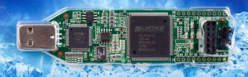
 Earlier this year, I showed you how to build a simple project with an inexpensive Lattice iCEStick and open source tools. (The iCEStick appears to the right.) Since then, I have wanted to come back and do something more practical. This time, I’m going to take a UART core from GitHub and use it to talk to the PC via the USB port on the iCEStick. Then I’m going to build a custom PWM block from scratch and create a PC-driven PWM peripheral. Along the way, you’ll see some Verilog nuances like parameters and get some more hands-on experience with using existing cores and working with test benches. Later, we’ll add multiple PWM outputs quickly by creating more instances of the PWM block.
UART Communications
As much as I enjoy building everything from scratch, I also know I can grab some common building blocks to make things easier. Sometimes I reuse my own code, and there are other places to look, too, including:
In this case, I knew the iCEStick’s USB port could act as a serial port on the PC, and a quick search found this GitHub repository. The UART is a thin wrapper around an open source UART that resides on OpenCores.
I have my own UART code, so if it were not for the iCEStick-specific wrapper, I would have probably used it. However, it was too easy just to download the UART ready-to-go. There is one catch: the project includes the underlying open source UART as a subproject. If you download the ZIP file from GitHub, that subproject will be an empty folder that you’ll need to fill in separately. If you clone the project, you need to initialize the subproject like this: git submodule update --init
The project includes a simple test driver that echoes characters. It is always a good idea to make sure that borrowed code works before you start adding things to it, so the first task is to download the test project to the iCEStick and get it working. In fact, for this simple project, I’ll start with the test code as a skeleton for the finished design.
If you need a refresher on Ice Storm (the open source tools for the iCEStick), you can check out my earlier post. The repository has a Makefile that will let you simply run make to build the project. If you type make flash to the command line, the makefile will build the project if needed and program it to the FPGA. Be sure the FPGA is plugged into a USB port.
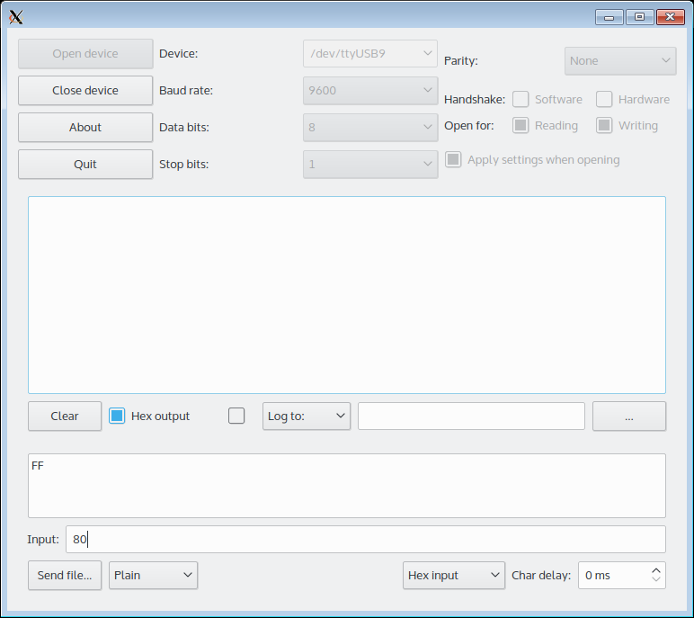 The FPGA will enumerate as a serial port — /dev/ttyUSBx under Linux. To talk to the FPGA, you’ll need to connect a terminal program to that port. For this step, any terminal program would be okay (e.g., minicom, picocom, or putty). However, when the PWM block is in place, you’ll want a terminal that can easily handle hex codes instead of ASCII characters. There are lots of choices, but I suggest Cutecom, which should be in your software repository (or download it from its homepage).
Once you have the port open at 9600 baud, you should be able to type characters in and see them come out. The uart_demo.v file produces the echo using an instantiation of the UART core:
always @(posedge iCE_CLK) begin
    if (received) begin
        tx_byte <= rx_byte;
        transmit <= 1;
    end else begin
        transmit <= 0;
    end
Just for fun, let’s convert lower case letters to upper case letters:
always @(posedge iCE_CLK) begin
    if (received) begin
        if (rx_byte >= 8'h61 && rx_byte <= 8'h7a)
            tx_byte <= rx_byte & 8'hDF;
        else begin
            tx_byte <= rx_byte;
            transmit <= 1;
        end
    else begin // else goes with if (received)
            transmit <= 0;
    end
There are lots of ways you could have written that, but I was going for clarity. In English, the right-hand side of the tx_byte assignment reads: If rx_byte is between 61 hex and 7a hex, inclusive, use rx_byte anded with 0xDF, otherwise just use rx_byte as-is. Change the code and flash the device again and verify that lowercase letters get converted to uppercase.
About PWM
With the UART working, we can move to the heart of the project: a Pulse Width Modulation (PWM) generator. There are many ways to generate PWM. Imagine you are standing by a light switch in a dark room. If you turn the switch on, the room lights up, of course. If you turn the light on for 1 second and then off for 59 seconds, the total light in the room will be 1/60th of the amount of light when the switch is on. Now imagine you can switch the light very quickly. So out of, say, 60 milliseconds, you turn the light on for one millisecond. Your eye will average the light, and it will seem like the light is very dim.
What if you wanted the light to be 50% as bright as the full on light? You have a few choices. You could turn the light on for 30ms and then keep it off for 30ms. This is called “equal-area PWM.” However, you could also turn the light on for 1 ms and then off for 1 ms, yielding “proportional PWM”. Which way is best? That depends on what you want to do. For example, having 1 ms pulses will probably make any light flickering less obvious. However, using proportional PWM means the frequency of the pulses changes based on the duty cycle, which could cause buzzing in motors at some speeds.
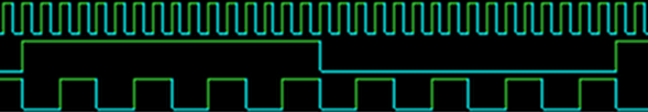
The picture below shows two 50% PWM signals. The top trace is the clock, the middle trace uses equal area semantics, and the bottom trace is a proportional PWM generator. Although the signals look different, both of the bottom traces are on half the time and off half the time.
I decided to create one block that can do either type of PWM. When you use the core, you’ll be able to pick which method you want it to use.
Creating a PWM Block
It is easy to generate PWM outputs by just driving a counter with the number of bits of resolution you need. For equal-area PWM, you can start with the output on when the counter is zero. When the counter reaches the duty cycle you want, flip the output off. For example, with an 8-bit counter, a roughly 50% duty cycle would be a count of 127. The output would be high on counts 0 to 127 and low from counts 128 to 255. You could trim the number of steps by resetting the count to zero early. For example, if you reset the counter at 200, then 50% would be 100, which is handy, if not necessary.
Proportional PWM is a little bit trickier but still easy. Sticking with an 8-bit resolution, the PWM generator can use an 8-bit counter with a carry output. On each clock cycle, you add the duty cycle value. That’s it. The output is the carry output of the counter. Consider a duty cycle of 0x80. Initially, the counter is at zero. On the first clock cycle, the counter will be 0x80, and since the carry output bit is zero, the output will be low. The next add results in a counter value of 0x00, but a carry occurs, so the output goes high. You can see this is going to repeat since the next cycle will be 0x80. That’s how the 50% duty cycle occurs.
If you work through the counter with a duty cycle of 1, you’ll see that there will be a large gap between high outputs. If you add 0xFF to the counter on each clock cycle, you will get almost constant high outputs.
I decided to create one block to do both styles. The Verilog interface looks like this:
module pwmblock #(parameter CNT_WIDTH=8, DIV_WIDTH=8)
    (input clk, input reset, input [CNT_WIDTH-1:0] increment,
     input [CNT_WIDTH-1:0] endval, input [CNT_WIDTH-1:0] match,
     input [DIV_WIDTH-1:0] scale, output reg epwm, output ppwm);
I’ll talk more about the parameters in tomorrow’s post. The arguments include the standard clock (clk) and reset inputs. The remaining inputs are:
increment– The amount to add to the counter on each clock cycle (1 for equal area; duty cycle for proportional)endval– The counter value that causes a resetmatch– The counter value that causes the output to toggle (the duty cycle for equal area)scale– A prescale counter for the clock (set to zero for no prescale)
The outputs are epwm for the equal area output and ppwm for the proportional output. You would only use one per instance, of course.
PWM Shortcuts
Setting up the PWM block for proportional or equal area mode just requires setting the right parameters and picking off the correct output. However, to make it easier, I created two wrappers that only expose the arguments you need for each mode:
// Handy wrapper for equal area
module epwmblock #(parameter CNT_WIDTH=8, DIV_WIDTH=8)
  (input clk, input reset, input [CNT_WIDTH-1:0] endval,
  input [CNT_WIDTH-1:0] match, input [DIV_WIDTH-1:0] scale, output pwm);
  pwmblock #(.CNT_WIDTH(CNT_WIDTH), .DIV_WIDTH(DIV_WIDTH))
  pwmb(clk, reset, 1, endval, match, scale, pwm,);
endmodule
// Handy wrapper for proportional
module ppwmblock #(parameter CNT_WIDTH=8, DIV_WIDTH=8)
  (input clk, input reset, input [CNT_WIDTH-1:0] duty, input [DIV_WIDTH-1:0] scale,
  output pwm);
  pwmblock #(.CNT_WIDTH(CNT_WIDTH), .DIV_WIDTH(DIV_WIDTH))
  pwmb(clk, reset, duty, 0, 0, scale,,pwm);
endmodule
Unless you need something special, you’ll probably use the wrappers.
Test Bench and Simulation
Although it is tempting just to try to load code into the FPGA for testing, unless it works the first time (yeah, right!) it is much more efficient to develop the system in a simulation. I use EDAPlayground to test the PWM code. To exercise it, I needed a testbench that is just a simple driver to use the block and generate some results you can compare to what you expect.
You can find the testbench and code on the EDAPlayground site, and you can run it there, too. Here’s what the testbench looks like:
`default_nettype none
module test;
reg clk=0, reset=1;
wire ep, pp, ep0, pp2, ep1;
always #1 clk=~clk;
// 10/256
epwmblock dut0(clk, reset, 8'hff, 8'h10, 8'h0, ep0);
// 10/1024
epwmblock #(.CNT_WIDTH(10)) dut1(clk, reset, 10'h3ff, 10'h10, 8'h0, ep);
// 255/256
ppwmblock dut2(clk, reset, 8'hFF, 8'h0, pp);
// 128/256 with prescale=1
ppwmblock dut3(clk, reset, 8'h80, 8'h1, pp2);
// 16/32
epwmblock dut4(clk, reset, 8'h1f, 8'h10, 8'h0, ep1);
initial
begin
  $dumpfile("dump.vcd");
  $dumpvars(3);
#5 reset=0;
#4096
  $finish;
end
endmodule
The testbench isn’t hard to understand. It generates a clock and just wires up a few test devices, recording the results for a few thousand clock cycles. Here’s a partial run of the simulation:
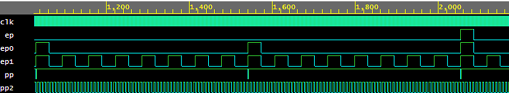
You can match up the signal names on the left to the testbench code to see the PWM duty cycle for each trace.
Next Time
This example is almost too simple, but it is also a lot to digest. Next time we’ll integrate the PWM and UART on real silicon, add some channels, and make the protocol a bit more sophisticated. Along the way, you’ll get to see how Verilog handles arrays and parameters. If you want a refresher on how to use EDAPlayground to do simulation, check out the videos from the last time I talked about the iCEStick, including the video below.


I would highly recommend named instead of ordered parameters. It avoids mistakes, and makes the code much more readable.
There’s still a lot of code examples that don’t do the 2001 standard that introduced the named parameters. But it is nice, and I imagine all the tools we are using does use them. A good paper on that: http://ocw.mit.edu/courses/electrical-engineering-and-computer-science/6-884-complex-digital-systems-spring-2005/related-resources/parameter_models.pdf
“There’s still a lot of code examples that don’t do the 2001 standard”
I agree, so let’s not create more. :)
You could turn the light on for 30ms and then keep it for 30ms. This is called “equal-area PWM.”
Keep it what? On? That’s not PWM, that’s on… Probably better to do an example with a different duty cycle than 50%, otherwise they just look identical, but with a faster pulse cycle…
The missing word was off. Same pattern as in the 60 second example right before. Fixed.
Cool. I was actually trying to point out that your image, or explanation, don’t really seem to be a good depiction of two different types of PWM… they both look like fixed duty cycle (50%) with two different frequencies to me, which is one type of PWM. The two other types I know of are fixed frequency with a variable duty cycle, and fixed pulse width with a variable frequency.
The difficult part of FPGA work is thinking in multiple dimensions – namely time. If you needed 10 independently programmable PWMs, what would you do? Not as simple as instancing 10 of your defined Verilog modules if you are constrained on logic area. Functional interleaving, gate-rating, pipe-lining and other concepts involving a time dimension are the hardest concepts to wrap one’s head around in programmable design; and usually where 99% of errors are made.
I was going to echo that comment when I saw “If you need 20 PWM blocks, they will also run at the same rate as a single block.” because, while it can sometimes be that simple, unless you have an awareness of what logic is being synthesised and how the FPGA is utilised, one can rapidly hit issues where there’s no space to synthesise the requested logic and the desired speed without some time/logic/puzzle hoops being jumped through to keep the end result.
I think that having one PWM module that performs two types is too clever for teaching purposes, and needlessly complex for real use. It would be more straightforward to have two separate designs. Easier to understand, and possibly more efficient to implement.
Also, pick a consistent indenting style, especially when you have so many if-else statements. For instance, the ‘else’ in line 33 goes with the if on line 32, but that’s not obvious from the indenting. This is especially important if the goal is to teach beginners.
What is the maximum PWM frequency on this particular FPGA?
That depends on a few factors, such as bit length, PWM design, pin allocation, and how much other logic you have (the fuller the FPGA, the harder it will be to find good routing).
Rough guestimate is somewhere between 100-200 MHz. Best way is to run the design through the tools, and do a static timing analysis.
Thank you. I was thinking about the sine wave signal generation at high speeds, by continuously changing the pulse widths, and using the low pass filter after. So this might be the tipping point to convince me to buy my first FPGA.
Keep in mind that the PWM frequency needs to be quite a bit higher than your target frequency. Suppose you manage to get a 256 MHz clock, and use 8 bit PWM, you only end up with 1 MHz at the end. Even less, because your filter won’t be perfect. Also, any digital noise from the FPGA will be superimposed on the signal.
For generating sine waves, it’s easier to use a proper DAC. For audio frequencies, there are cheap I2S audio DACs with all the filtering already built in.
Yes, DAC might be better. Options, options … I’m thinking whether to buy an FPGA from this article or some other model to get me started :) It needs to work well in Linux though.
my “goto” PWM solution in TTL has always been an 8 bit counter that free runs from a clock source, the outputs from the counter go to the “A” inputs of 2 74xx85, 4 bit magnitude comparators cascaded together, tie the “B” inputs to “Hi” or “Lo”.
The PWM signal then comes out of the A>B or A<B output.
Watch out for x-prop issues in code like:
always @(posedge iCE_CLK) begin
if (received) begin
transmit <= 1;
end else begin
transmit <= 0;
end
If 'received' goes X (unknown), rather than transmitting on that unknown through transmit, in this scenario, transmit will be 0 (the 'if' condition effectively performs a "is received exactly equal to 1" which it isn't because it's X). It's an easy way of missing issues in simulation that cause problems in the real code.
Also, in the code sequence immediately below this one in the article, what is the expected value of 'transmit' when converting to upper case? (it's set to '1' when passing through a byte and '0' when nothing is received, I would expect the synthesis tools to infer a latch and only 'transmit' an upper case character if it followed in the adjacent clock cycle with a byte that was sent)
Not a latch but a flip-flop, and transmit would be 0, assuming that the ‘received’ signal is only high for a single cycle after each received character.
It’s a clocked process so they’d all be flops (transmit and tx_byte) – my apologies, I was using the shorthand of ‘latch’ in the context of flops as being a flop that holds the value into other subsequent clock cycles (a clocked latch). In this case, transmit will hold the value from the last cycle when performing a conversion to upper (it may be that it’ll be ‘0’ by virtue of never having ‘receive’ high in multiple adjacent clock cycles).
I see. It is quite common to forget a case/if-else branch with conditional logic, and end up with a inadvertent latch.
Your list of use cases misses the most important one I’ve seen FPGAs applied to in my professional career (defence): signal processing. The ability to inhale data at tens of Gbps and do complex number crunching on it is fairly unique to FPGAs. If you want to build a high performance radar or radar-countermeasures system, phased array beam-steering, MIMO anti-jam pre-processor, etc… you do it in an FPGA. Likewise lots of radio communications are implemented in FPGA – think of what you can do with consumer-grade SDR then crank the bandwidth and complexity by a few orders of magnitude.
That’s under Why Use an FPGA:
> An FPGA’s ability to run at high speed and in parallel makes it an excellent choice for parallel processing and high-speed signal processing.
Most of my FPGA work these days is rad hard stuff.
What’s the point of the proportional PWM in the example?
There’s also the case of phase-corrected PWM which has to be symmetric around the clock signal, or else you get frequency modulation as you change the duty cycle and that shows up as EMI issues. Suppose you change the duty cycle of the naive counter PWM by 1 every cycle – the midpoint of the waveform shifts relative to the clock cycle, which means the signal phase starts to lag or advance the clock signal, which means the output frequency is different from the clock frequency for as long as you keep changing the duty cycle.
fpga4fun.com has neat examples
If you’re using a FPGA for PWM, wouldn’t it make more sense to do something more advanced like Delta Sigma? In other words, something that cannot be done with a classical microcontroller.
The ‘proportional PWM’ described in this article is Delta Sigma.
Absolutely! There’s a lot of discussion online regarding “PWM vs. Delta Sigma DAC” and an interesting app-note http://www.ti.com/lit/an/slyt076/slyt076.pdf
I wish I hade done more on that topic, you should be able to get a comparable effective number of bits at significantly lower clock rates. The theory that goes into implementing a proper delta sigma DAC however is something that is sure to quench interest in beginners.
Perhaps Jeri can help, https://www.youtube.com/watch?v=DTCtx9eNHXE
Thanks for this series of articles. I like that the new material is coming fast enough to be interesting but not so fast as to be overwhelming.
While I appreciate the comments pointing out technical subtleties, I think it’s important to remember that goal is to get beginners to do something with FPGAs. I don’t think it’s important that “something” be optimal or even practical. For a topic as complex as FPGAs just getting started is a worthy goal.
I had a PSOC 5 dev kit lying around, and because of this article I made my first blinker in verilog! I always considered PSOC the gateway drug to FPGAs, but I had never actually looked into it, that’s done now. I have the worst PWM timer ever blinking an LED (no reset, no division, and I suspect the output is one tick late on the input).
Thanks!