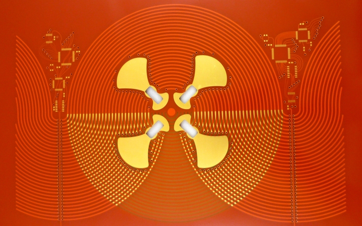
Recently I’ve been getting curious about interesting PCB shapes. In the past I’ve always used simple Polygons, perhaps rounding out the corners to make the design a little more aesthetically pleasing. The board to the right was my introduction to the possibilities of oddly shaped boards. It’s designed to couple with a piezo buzzer (used as an actuator). I’ve been planning to have it fabricated out of FPC (Flexible Printed Circuits), but with fabrication being so cheap I sent it to OSHPark to see what they’d make of it. OSHPark doesn’t have hard specs around internal routing, but in my experience they’re up to try anything (and they’re quality is always great). The width of the prongs on the PCB shown is 5mm. I figured it was a risk, and that it was likely the FR4 could break, but it came back great!
This has led me to the realization that my boards could look much more exciting than they do currently, and that our highly optimized modern PCB fabrication process provides a lot of room for experimentation. This article will discuss some of the options available when creating non-traditional PCBs.
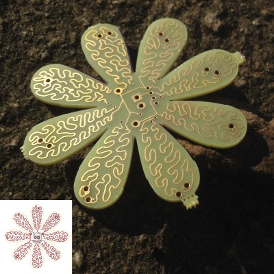
The board to the left is for a simple solar lantern. The LEDs sit on the end of the wiggly tracks, with the driver IC sitting in the center. I designed it to try and push the process, see if a PCB could be made to look a little less sterile and more like a craft object. The traces going to the LEDs were left unmasked, to allow them to come out in gold with ENIG. I think the fabricated board looks ok, but for the next revision I’ll retain more mask, which should make the traces stand out. Gratifyingly I now have an even better idea of the weird board shapes OSHPark can cope with (and will try and push the process even further).
Most layout tools, KiCad included, are not designed with the fabrication complex edges or components in mind. While the edges in the coupler above were created in KiCad it was an unpleasant process. So for the solar lantern I opted for external tools.
First, I designed the flower shaped edge cut in Inkscape. In recent versions of KiCad it’s pretty easy to import the edgecuts. Firstly create your edges in Inkscape, ensure that the design is a simple line drawing and save it as a DXF file. Then just select “File->Import->DXF” in KiCad, and import the DXF into the Edges layer.
Creating wiggly traces in KiCad is more difficult, in fact it’s not possible. KiCad has no concept of non-straight traces, and limited pad geometries.
KiCad incorporates a tool called “Bitmap2Component” while many have used this to good effect to add logos to their boards it’s not ideal when working with vector image data and has limited functionality. To solve this shortfall we look to svg2mod. This tool allows you to convert an svg into a KiCad footprint using a simple command line tool. On Linux you can use it as follows:
./svg2mod.py -i ~/design.svg -o ~/design.mod -p 0.1
As KiCad only uses straight lines, the curves in your original svg will be broken down into straight line segments. The “-p” parameter determines how many segments a curve is broken into, and may require some experimentation. svg2mod works with layered svg files. You can create separate layers in your svg for copper, mask and silk, producing complex component footprints. For the PCB above I used this to remove the mask from all the wiggly traces. Eagle users may want to check out svg2poly which appears to provide similar functionality.
This is my first attempt at creating more aesthetically pleasing boards, but Saar at Boldport has been making great looking PCBs for years.
Some of his designs (like the one shown to the right). Are hardly recognizable as a slab of FR4. Marie Claire commissioned this and other boards like it for a photo shoot called Haute circuits, which used the boards as a backdrop for pieces of luxury jewelry.
Boldport’s designs are always unique and beautiful. Characteristically, there’s never a straight trace to be found. Producing such designs in a traditional layout package would be almost impossible.
For this reason Saar took the audacious step of designing his own layout software from scratch. The tool is called PCBMode and is free and open source. It’s very much designed for Saar’s unique workflow and takes a little getting used to, but is worth checking out.
Rather than having its own interface PCBMode schematics are represented in a series of JSON files. These are then processed into an SVG which can be edited in Inkscape to produce an aesthetically pleasing design. The svg is then finally processed to create gerbers ready for fabrication.
PCBMode produces beautiful boards, but takes a significant investment of time to get used to. If you enjoy PCBMode’s beautiful boards, you might want to check out Saar’s beautiful kits which he’ll be providing on subscription starting in March. All lovingly designed in PCBMode.
There’s one more time honored tradition we should mention, albeit with a modern twist. Before the rise of computerized layout tools, it was of course pretty common to layout boards by hand.
These old boards with their wildly irregular (generally maskless) tracks still have a certain visual appeal. For hackers etching at home this is of course easy to replicate. But you can also accomplish a similar aesthetic using a commercial fab and a tool to convert svgs directly to gerbers.
For this purpose Cenon works well.. You’ll have to separately create and convert svgs for each layer and edges. You’re also left with the problem of creating your own drill file. Of the processes I’ve investigated so far, svg2mod with KiCad works best for me, allowing you to easily create complex, multi-layered vector component footprints in Inkscape to be imported into KiCad and combined with more traditional circuit elements. The process of creating and importing footprints and edges works well, even if it’s a slightly clunky process.
I’d love to hear about your favorite innovate PCB layouts, and any tools you’ve found to aid in the process of designing novel PCBs. Please comment below!


Reminds me of the practice of watchmakers in the past decorating the interior of their pieces in places that would only be seen by other watchmakers when the unit was being serviced or cleaned, but almost never by the owner.
Check out brainsmoke’s deltoidal hexecontahedron:
https://wiki.techinc.nl/index.php/Polyhedrone
Which is basically a giant mesmerizing LED-filled pcb.
Cool. Didn’t I see Luke Skywalker swatting a light saber at one of these on the Millennium Falcon?
https://wiki.techinc.nl/index.php/File:FullSizeRender.jpg
https://wiki.techinc.nl/images/5/55/FullSizeRender.jpg
I’m actually not that big of a fan of curvy traces. To me more aesthetically pleasing are 45 degree cornered, straight lines. Only place I see my self of doing something more out of usual, is to make the PCB silhouette in a fancy shape
I recently tried out Saar’s PCBmode, and the learning curve is steep, especially for someone like me who’s never been good at scripting and code. But after the initial hiccups, it gets easy and the results are awesome. It would be a great tool in the hands of an Artist, unconstrained by the limits of traditional EDA.
Another interesting tool I found is VeeCad (http://veecad.com/) which “takes a schematic generated netlist and assists you to build a layout – on strip (Veroboard), matrix, donut, tripad, Atarado Smart, and other prototyping boards.”
http://veecad.com/shot_connective.png
Yea I think PCBmode is really cool. I want to invest a bit more time in playing with it!
How dare you omit Yuri Suzuki’s tube map radio?! I mean, ok, it’s a fairly typical PCB, but… Uh… Reasons.
http://yurisuzuki.com/news/tube-map-radio-is-now-available/
that is neat
http://hackaday.com/2015/04/02/tube-map-radio-and-denki-puzzles/
The wiggly hand-drawn traces of old PCBs, including some old computers, definitely provide a sharp demarcation between the old days and the modern day. All of a sudden everything went square, computer-generated. It’s nice to think, now technology has advanced even more, we can even consider aesthetics in PCB layout, even though, as DV82XL said, most people won’t ever see them.
It would great to see more support to model bezier curve traces in layout tools. I guess the likes of Altium must support this. PCB fabrication feels like an amazing resource capable of rendering complex layered structures at low cost and that theirs a lot that could be done with it aesthetically.
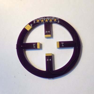
I made some circular boards for an Inductively powered, frequency controlled RGB LED:
http://youtu.be/kgYtYXVkan0
Although the traces are aestheticly pleasing, they are integral to the circuit. ;)
Really nice! I think making functional elements on board is really interesting. I’ve been looking at some odd round boards myself:
http://41j.com/blog/2016/01/notes-1612016/
The plan is to drive them with around 10kv and see if they will work as electrostatic motors. I’ve run none of the force calculations though so no idea if it will work. I think you should also be able to build rotary/linear motion sensor this way too. Cheap digital calipers seem to use that mechanism.
There’s an artist I really like called Lumen Electronic Jewelry, which makes PCB art. Her designs are solar powered blinking necklaces and earrings (with a supercap to store charge for a few hours), and all the components and traces are functional. The circuit boards are in all kinds of shapes, and she has kits at different skill levels of soldering. Her pieces are really worth checking out: http://lumenelectronicjewelry.com
Great introduction, thank you!
I have been wanting our PCBs to look less sterile and devoid of any imagination for some time. This points me in the right direction.
Cheers
My latest board is designed to be a snap-together 3D quadcopter (by ‘snap together’, think of those wooden dinosaur skeletons you made as a kid). The board edges were made in QCad and imported to KiCad via the Import DXF function like in the article. It’s not artistic like some of the examples above, but the complexity of the outline is much more than I had ever done before:
See https://hackaday.io/project/8488-chiindii for more details
Gah, I have no idea how to link an image into comments… here’s the link:
https://cdn.hackaday.io/images/9104501447880651978.JPG
OK, so I guess just putting a link is enough… no tags needed. Anyway it’s there now… :-)
Oh cool. I’ve been looking at those too and modeled a CX10 style enclosure:
http://41j.com/blog/2016/01/3178/
Was planning to make a CX10 compatible board so I can use the same plastics if I wanted to. Interesting, you can buy packs of the rotors on eBay which should make life easier. You can also buy bare boards from Shenzhen like this one:
http://41j.com/blog/wp-content/uploads/2016/01/bareflyer.jpg
From here: http://world.taobao.com/item/18839984356.htm
I’m thinking of getting a bunch of those to play with they look fun! I really like your design though, using slotted PCBs to build a more complex mechanical structure is cool!
I’m not a fan of artistic PCBs.
Why? Because artists seem to think that everything is their canvas, ready for their expression. While this is not wrong per se, it annoys me to no end when artists ignore the properties of the technology and materials they’re working with.
Electronics are complicated. Design rules exist for a reason. EMI, signal integrity, power consumption, noise floor, etc. Layouting a PCB is an art in itself if it just needs to work. However, when you reduce this to “look at his designs, they’re so beautiful because they use crazy outlines and squiggly traces,” you ignore the price this comes with: A non-working circuit. Strange outlines promote mechanical stress, which drastically decreases reliability of solder joints and SMD capacitors. Long traces without proper ground planes decrease noise immunity and increase noise emmission, making the circuit less reliable. I have little respect for any artist who thinks they can just use their artistic freedom everywhere. I have the utmost respect for all artists who learn about the technology and the limitations and then make art while still retaining functionality. This might not be especially relevant for decorative art such as pictures, but when you’re talking about art that’s supposed to serve some function or has the potential to affect other devices or people around them (buildings, electronics, …), I find it absolutely imperative to work with the technology. To clarify my point: If a house you build looks great, but is completely unusable because you couldn’t be bothered to find out why conventional houses are designed and built the way they are, you’ve failed utterly at being an architect AND an artist.
You must be fun at parties.
I’m not an artist, but I think that sometimes art for art’s sake is perfectly fine. And why the heck should you care if someone else’s circuit doesn’t work as well as you think it should?
Kudos to all of the circuit designers that create these beautiful works of art. Double kudos to those that create PCBs that are functional AND look great.
I’m sorry that you see the world around you as an engineering problem that can only be solved with rigorous technical expertise and universal design constraints. I’ll be sure to put all of my “messy” diy synthesizers away and cover up my projects in smooth, featureless enclosures so I don’t offend you.
Good points all. But developments towards more aesthetically pleasing circuits just pushes the medium and expectations from experts, especially where the circuit is the primary/sole product… At the cost of confounding novices with buggy circuits. Maybe if we encourage people to view this style of design as extremely difficult to pull off correctly, rather than just with disdain, novices will approach it with caution.
Side effect of “artistically” supportive software: “My circuit is buggy, halp!” posts requiring a picture of the PCB before continuing.
The people nay-saying this comment are people who have probably never ventured into higher frequency design. The artistic approach to circuit design is all fine and dandy if you’re using components with long rise times and/or slower frequencies (<100 MHz rule of thumb). Once you get into the faster circuits the "invisible" half of the circuit (read as: "ground" [AKA current return path]) starts to matter a lot more than people think. If you're trying to make a manufacturable product that can be sold, EMI/EMF/EMC starts to be a huge concern as makers run the risk of violating cert requirements (another topic that isn't discussed enough if at all these days).
While I can understand the spirit and principle behind the poo-poo-ers, those feelings simply don't scale if you want to build higher end products in any meaningful way. Keep preachin', it's an important message.
Let them fail and hopefully some of them would learn it the hard way. There is no point of saving their butt when they don’t appreciate your efforts.
Yes but the comment people are replying to was far more absolute than that. ‘f’ starts right out with “Im not a fan of artistic PCBs.” Then he/she pretty much goes on a rant about it. At no point does ‘f’ talk about high frequencies. Look at the examples given.. a solar light, a piezo coupler… nobody is talking about building fast computers or high bandwidth modems. Even if you were building such a circuit there are portions of the circuit where it matters and portions where it does not.
I don’t think there is any reason to worry that makers will get so artsy that all they ever do is pop out boards that do not work. Certainly some will try things that do not work. When they do that is a learning experience which will lead to something better the next time. It’s not even a failure if learning experiences are what they are after in the first place as fits a site called ‘Hack-a-day’. This is not exactly ‘Commercial Industrial Design Journal’ is it?
There are many opportunities to do problematic designs even with pretty run-of-the-mill stuff.
For example, you’d probably want to have switching regulators for your energy-efficient LED lighting project, i.e. “solar light.” Switching regulators are notoriously hard to design in a way that makes them fulfill EMI regulations. For lighting applications, you’d want lowest cost and maximum conversion efficiency, while output ripple and noise are not very important. There are one-chip solutions with a couple of passives that can provide a boost SMPS from a single battery to drive white LEDs. Given this, I do suspect that some people who are not super-knowledgeable about everything might be inclined to include such a chip on their PCB. Which is great, as they are really easy to use. However, if you connect the output of this chip to a trace, the trace will act as an antenna and radiate RF energy. Usually, this is not a problem, as only a couple of centimeters of trace are connected to this chip. If you want to be all artistic and connect half a meter of squiggly trace between the chip and LED, you’ve just built yourself a nice antenna. You might think this is fun, but people who will get degraded performance of their equipment due to the interference your artsy circuit generates will not think so.
A signal with a frequency of couple of MHz, carelessly routed and not slew-rate limited, is usually enough to cause massive interference. It will of course also cause massive interference in your own circuit, which will have degraded performance.
To be precise: Yes, the 1 MHz PWM so you can make 5 meters of LED string breathe, which you’re able to do on an Arduino with a couple lines of code is creating EMI to no end.
Analogue designs need a good layout. It can be beautiful, but the most important thing is that it works.
However, it’s no problem to build artistic PCBs. It’s just the way “artists” approach this that bothers me to no end. The correct way is this: 1) Learn about what you’re working with, its properties and limitations. As a good artist, this should be about 80% of what you’re doing anyway. Get to know how to make functional PCBs, ignoring the artistic aspect. 2) Now make art. Having learnt so much about the properties of the material you’re working with (PCBs, electronics), you can make beautiful art that still works well, instead of an electronics collage with voltage applied to it.
I work in a highly artistic environment (creative technologist at a marketing agency) and get a lot of flack for my “cardboard prototypes” and “plain looking documentation”.
Make it work, then make it pretty (if there is time).
F you are spot on whether or not people agree. As someone who goes all the way back to the bishop graphics days of taping boards, a true piece of PCB artwork is aesthetically pleasing while also meeting all EMI, ESD, and EMC requirements. I could make a board look really cool by placing all the decoupling caps in a neat row, but then again, don’t they belong near what they are supposed to be decoupling?
Even cooler looking than PCB artwork? Integrated circuit artwork.
There’s a fairly popular local art installation that makes use of a number of LEDs and (IIRC) Arduinos networked together. Even though it was meant to be temporary, weather got to the LEDs and ruined them forcing a repair about half way through the exhibit. It proved really popular so the exhibit is being rebuilt again for a permanent install.
Even as a temporary install the artist should’ve realized the elements would ruin his work. I don’t want to think about the RF interference here.
Then there’s Steve Jobs…. http://gizmodo.com/5575412/apple-design-vs-apple-engineering
It depends. Yes, if you want a functioning circuit there are laws of physics you can’t ignore. For simple circuits though there aren’t many limits. To produce a functional, and attractive bit of high-performance PCB would take real genius.
This. For a number of years not so long ago I taught embedded systems — “physical computing” in a Digital Arts program at a local university. The level of wilful ignorance — not with the students, but the staff — was staggering. The whole principle of the course was that engineering had something to teach art, except nobody was willing to learn how to use the engineering and technology effectively or learn how it worked or how it came to be and what could be learned from that. They just wanted “plug-and-play” solutions, which invariably meant plagiarising code from all over the place (this is the staff I’m talking about here – so-called “professional artists”). Grrrr.
And don’t get me started on “creative technologists”…..
Any MS Windows alternative PCBModE or Cenon?
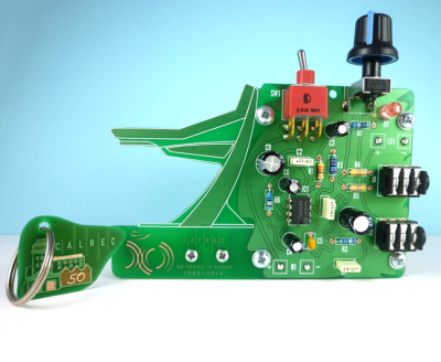
What is the board pictured at the top of the article?
That’s one of the Haute circuit boards from Boldport:
http://www.boldport.com/blog/2015/11/25/haute-circuits
The Piezo actuator board at the beginning of the article. I’m fascinated by tiny actuators, please elaborate
Ah, I just went and checked out your blog and I see you are working on an AF Microscope, which clarifies the purpose of the Piezo actuator. I’m more interested in piezos for high accuracy rotary/linear positioning, but still interesting. Thanks for the article, I definitely think there is a place in PCB design for beautiful/functional layouts. They can even help us humans to read a circuit better I think.
Ah, that explains it. I wasn’t able to visit that page yet because my work WSA blocked it as porn…
I once had to make a board that is now used as a tamper-detection device. It’s rectangular, because it has to, and is basically just a pair of traces running all over the board while avoiding some holes where there are screws mounted thru it. It’s something around 450x550mm big, and the traces are 0.5mm with 0.5mm spaces. While drawing it and checking fabrication outputs and all that i sometimes felt like it’s some kind of hypnotic pattern or one of those “magic” pictures you can see 3D shapes in when you look at it the right way.
And wasn’t there a T-Bone Cape for the Beagleboard that looked like a Ribeye Steak? Not really practical, but i guess someone had a laugh while trying to get that kickstarted.
Dude that works at Shadow Robotics has been working on a program for routing PCBs in a non traditional way. It seems to focus on laying down traces that are nice smooth curves etc. Check his site for a better explanation:
http://www.liquidpcb.org/
Thanks for posting that, it looks really nice, will check it out.
Altium is the package I use, and you can do amazing things with it. Is it expensive. Not for business, but for a hobbyist? Out of sight on price. You can drag matched pairs around and it automatically adjusts them. There are hundreds of cool things about this package. Its a far cry from taping using bishop graphics tape and doing a 2X camera reduction.
My dyslexia is acting up again, I clicked on this article to see beautiful and bazarre broads!
B^)
here’s one of my favorite boards, which i built back in 2013:
http://www.latentlaboratories.com/timeline/2014/8/5/2014/8/5/printed-cubist-board-1
broken link, here’s an actual working link :-/
http://www.latentlaboratories.com/timeline/2014/8/5/printed-cubist-board-1
I have to mention the awesome Badge from the last Hackaday SuperCon. That was really cool.
https://hackaday.com/wp-content/uploads/2015/11/72ejpm5nocvcoqoemv74_fmzesqkcpxiqv70jyc9psg1.jpg
http://i.imgur.com/F5r5wpx.jpg
Any link to the files for that flower by chance?
Hey, I built up the design, but it required a bodge wire. Once I’ve revised the board I’ll post the gerbers somewhere.