I’ve worked with a lot of students who want to program computers. In particular, a lot of them want to program games. However, when they find out that after a few weeks of work they won’t be able to create the next version of Skyrim or Halo, they often get disillusioned and move on to other things. When I was a kid, if you could get a text-based Hi-Lo game running, you were a wizard, but clearly the bar is a lot higher than it used to be. Think of the “Karate Kid”–he had to do “wax on, wax off” before he could get to the cool stuff. Same goes for a lot of technical projects, programming or otherwise.
I talk to a lot of people who are interested in CPU design, and I think there’s quite a bit of the same problem here, as well. Today’s commercial CPUs are huge beasts, with sophisticated memory subsystems, instruction interpreters, and superscalar execution. That’s the Skyrim of CPU design. Maybe you should start with something simpler. Sure, you probably want to start learning Verilog or VHDL with even simpler projects. But the gulf between an FPGA PWM generator and a full-blown CPU is pretty daunting.
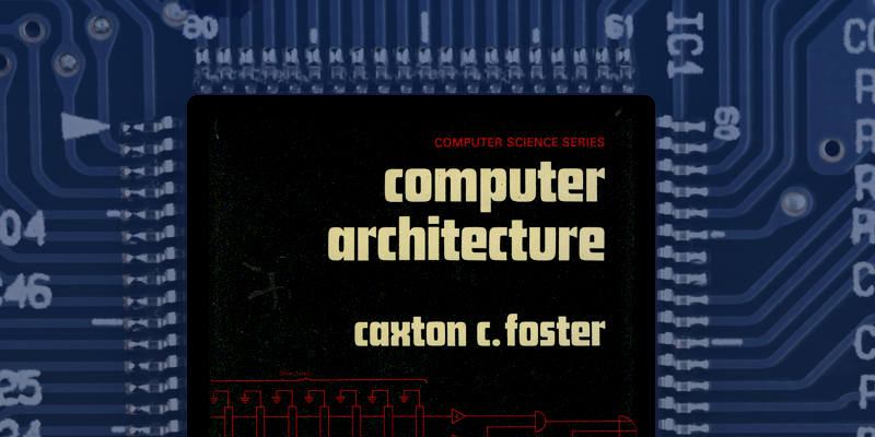
![[Image Source: Amazon]](https://hackaday.com/wp-content/uploads/2016/03/computer-architecture-book-cover-caxton-foster.jpg)
Getting the Book
There is bad news and good news. The bad news is the book is years out of print. The good news is that the book was so popular as a college text that it is easy to find gently used copies in the usual places (hint: Amazon).
There are several editions, but my remarks will be about the second edition because that’s the version I have. There are probably minor differences in Blue depending on the version. However, you don’t want to copy slavishly Blue, just draw inspiration from it.
The book should give you an appreciation of hardware description languages like VHDL and Verilog. Foster’s book predates these and uses good old logic diagrams. That’s good for learning, but you can see how unwieldy even a moderately complex CPU is in logic gates.
How it Works
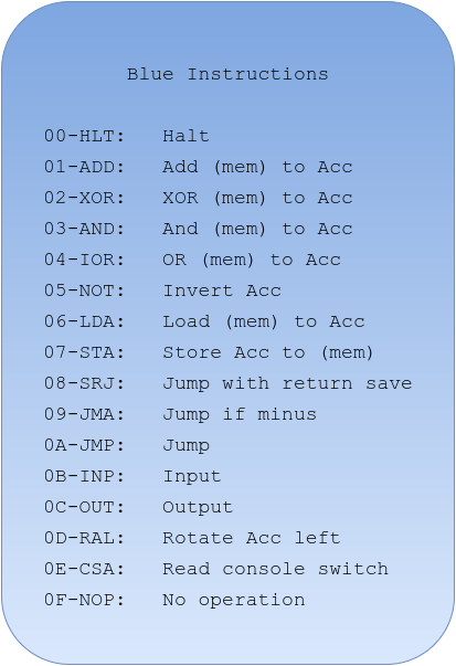 Foster’s Blue computer has a pretty typical architecture of a minicomputer from the 1970s (like a Data General or Digital from those days). A 16-bit word memory serves as a unified data and instruction storage with a maximum of 4K words (most of its commercial counterparts could handle 32K). There are a handful of instructions (well, if 16 is a handful; see right), which each use two major cycles: fetch and execute. Those major cycles divide up into eight clock phases each.
This is why this type of CPU is a reasonable place to start on your way to designing the next great supercomputer. Avoiding things like pipelines and multiple instruction issue let you focus on the core principles. These principles are at the heart of every CPU, even those that have many other details obscuring their fundamental operation.
For Blue, there are multiple resources: registers, memory, the accumulator, an arithmetic logic unit (ALU), the program counter, I/O, etc. All of these things connect to a common internal bus. Some things can only drive the bus (like the output of the ALU). Some things only read from the bus (like the memory address register). Some things, like the accumulator or memory buffer register, do both. The control unit orchestrates all these resources by enabling one device to write to the internal bus and at least one device to read from the bus in a given cycle.
The internals are very simple, especially compared to a modern CPU. Here’s a pictorial view of Blue’s internal structure:
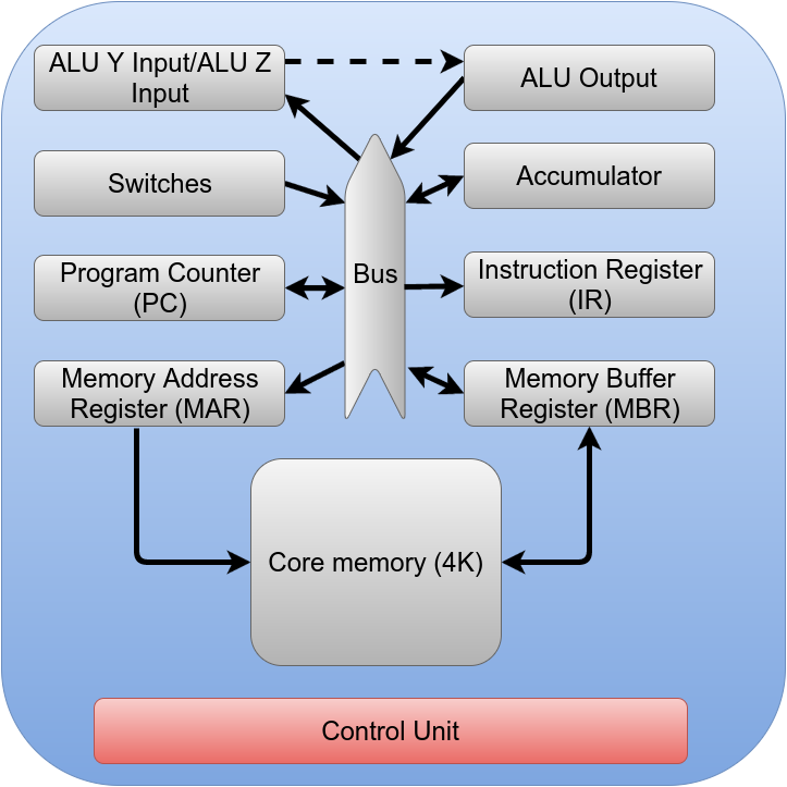
The control unit’s job is to read instructions from memory and then, based on those instructions, move data from one resource (for example, the memory) to another (for example, the accumulator). You’ll notice the dashed line between Y and Z and the ALU. That’s because Y and Z are actually the inputs to the ALU. The outputs include things like the sum of Y and Z, the inverse of Z, and so on.
The basic scheme for fetching instructions is this (Foster numbers from 1, so I will too):
- Fetch 1: Program counter (PC) to bus, load memory address register from bus, load ALU argument Z from bus, do memory read
- Fetch 2: Put constant 1 on the bus, load ALU argument Y from bus
- Fetch 3: Wait for memory access
- Fetch 4: Put Z+Y on the bus, load PC from bus
- Fetch 5: Load memory to memory buffer register
- Fetch 6: Put memory buffer register on bus, load instruction register
- Fetch 7: Available
- Fetch 8: Available
I omitted some details that don’t apply to modern systems. For example, part of the Fetch 5 cycle is to rewrite the data to Blue’s core memory. This is unnecessary for modern memory systems.
The Fetch cycle’s job is to read the instruction at the program counter and increase the program counter by 1. Fetch 1 is a good example of where the control unit does two writes in a single subcycle since the program counter has to go to the memory address register and Z.
For simple instructions, execution can occur in Fetch 7 and 8. Those instructions can fit in a single major cycle and don’t require an execute cycle. For example, a NOT instruction inverts the accumulator, so Fetch 6 for that instruction could put the accumulator on the internal bus and load Z. Then the final Fetch subcycle can move the ALU output to the accumulator. Also, it would have to flag the control unit to start a new Fetch cycle instead of an Execute cycle. In Blue’s original design, the STATE flag controls this and, by default, there is never an Execute cycle. So doing nothing, in the case of the NOT instruction, is sufficient to meet the requirement that the next cycle is a Fetch.
Some instructions need more work, however. In those cases, the Fetch 8 subcycle will set STATE to “E” (for execute). This provides 8 more subcycles for the control unit to manipulate resources in response to the instruction. This is especially important for instructions that access memory since you have to have another memory access cycle that doesn’t fetch an instruction. With modern high-speed memory, you might be able to condense everything into the 8 phases of Fetch, but remember Blue had relatively slow memory that needed a refresh after a read. The final step in any Execute cycle is to reset STATE to “F” so that the next cycle is a Fetch. Blue doesn’t need it, but in theory, STATE could be more than a bit if you had instructions that required multiple cycles (so you could have Execute 0, Execute 1, and so on).
How does the control unit know what to do? Each instruction has a 4-bit opcode (bits 15-12), and the remaining bits specify an address (now you see why Blue can only handle 4K words of memory). Once the instruction is in the instruction register, decoding the top 4 bits determines what happens in the next cycles.
Implementation
You’d most likely implement logic in Verilog or VHDL (although, you could draw gates like Foster did, using a simulation package, or maybe you want to build this in Minecraft). The concepts are the same however you do it.
You’d take all 16 instructions and build Fetch cycles for them (and Execute cycles for the ones you need). Then you can create logic to do each of the actions required. All of these that are the same get merged with an OR gate and fed to the register or other resource to make it do what it is supposed to do.
The resources are simple. You load the bus into a register, or you gate the register out to the bus. The ALU does simple logic internally, but otherwise is just a register that doesn’t just write its input back out. All the “smart” part is in the control unit.
Consider phase 4 of a Fetch cycle. It is supposed to have the ALU gate the sum output to the bus and then also have the PC read from the bus (this is how the CPU sets the next fetch address). In Foster’s design, this is a single AND gate. One input is the F bit (indicating a Fetch cycle), and the other is CP4 (meaning the 4th subcycle). The output fans out to both the ALU’s sum output gate and PC’s load input.
Presumably, other things will want to gate the sum output (the ADD instruction) or load the PC (a JMP instruction) so those outputs will really go to an OR gate that connects to the resource in question (see figure, below). For example, the sum output gate will also connect to an AND gate that merges the AND instruction decode with the inverse of F (indicating an Execute cycle), and CP8. The same output will drive the accumulator to read from the bus (again, through an OR gate that merges all the things that signal an accumulator load).

When you look at it this way, the CPU is simple. Just a bunch of readers and writers on a bus and a state machine that enables different items at different times. The resources are sometimes called the CPU’s datapath, and the resources are functional units.
Out with the Old
I already mentioned the core memory features of Blue are hardly necessary today. There are a few other items you may have to (or want to) correct in Blue’s design. Fast memory allows you to optimize some of Blue’s cycles. In particular, you could read or write memory on each phase, if you wanted to. You could make the PC know how to increment itself so that the operation could share a slot with something that used the internal bus.
Probably the biggest change, though, is the clock generation. Foster uses a delay line to make the 8 phase clock. Modern designers don’t like to use delays like this for several reasons. First, component variations make it difficult to equalize short delays, especially across different machines. Second, components change with time and environmental factors, so delays like this would require careful design to be practical.
However, I think even Foster didn’t like that design. One of the exercise questions in the book challenges you to think of different ways to generate the clock. The most obvious, I think, to a modern designer is to make a clock at 8 times the require frequency and drive a 3-bit counter. Then decode the counter to 8 outputs. Alternately, you could use an 8-bit shift register and just cycle it on each clock pulse.
The I/O instructions are a bit dated. The instructions aren’t bad per se, as they just read or write from a device specified in the address field of the instruction (well, part of the field). However, the logic is set up for things like paper tape punches and readers. You’ll want to change that out. In my design, I simplified the I/O structure quite a bit.
What’s Next?
You might be wondering what a practical implementation of Blue looks like. I’ll save that for next time. However, the point of this shouldn’t be to copy my implementation in Verilog. It should be to do your own rendition of the architecture using the tool of your choice. There’s at least one bug in the Foster book (at least, in the 2nd edition) and you’ll need to modernize the design a bit. However, creating your own flavor of Blue is a great way to develop your skills as a CPU designer.
What would come next? Later chapters in the Foster book talk about Indigo, another machine that is similar but has more modern addressing modes (like indexed addressing). That has some value, but if you can work through Blue, you can probably figure that out on your own. There are other features that are fun tweaks (like interrupts, for example) but don’t really propel Blue closer to a modern design.
If you wanted to modernize your design, the next step is microcoding (Foster touches on this in Chapter 8). If you think about the control unit of Blue, it could almost be a little computer itself, running simple programs that manipulate functional units. That’s how most modern CPUs work. They develop the control until as a very simple CPU (practically like a stripped down Blue) and use that to implement the real CPU control. Some computers like the old HP1000 would even let you create your own instructions in microcode.
The other big enhancement Blue needs is pipelining. The idea behind pipelining is that fetching and executing can overlap. If Blue were pipelined then when the first instruction was in the CP8 cycle, the 8th instruction would be in CP1. After 8 instructions, the CPU would execute one instruction per minor clock cycle instead of one instruction per 8 minor clock cycles.
Sounds great, but there are details. For example, a store instruction might refer to a result that isn’t ready yet. Special logic has to catch this case and stall the pipeline. Conditional jumps cause problems too since you have to clear the pipeline when you jump to prevent instructions from completing that were not supposed to run. This is a real issue for conditional jumps where you might not know if you will jump or not for some time.
If you are looking for the equivalent to Blue that’s a bit more modern, I’d highly recommend [Jan Grey’s] XSOC from around 2000. It also uses schematics but has a Harvard architecture RISC CPU with pipelining. Still, that might be a better second stop on your CPU design journey. Next time I’ll show you a Verilog implementation of Blue. Until then, you might enjoy a terminal session with that CPU in the video below.


Cax Foster was head of the Computer and Information Science department at UMass/Amherst when I was a student there. Nice to see his book is still popular.
// Real Computers have switches and lights.
Great article Al. I love your knowledge filled tech articles!
Agreed, best one I’ve read in a while on HaD. But I do love computers lol.
Interesting article. But I have two tiny points:
1. Tell your students that are interested in game making to look up Unreal Engine 4. It’s free, its sources are available for everyone, it shows the results in real time and it’s scripting is based on flow charts. Should be easier for them to learn and use.
2. The third drawing, the one with gates would benefit from getting a bit of contrast. I see only gates and some lines…
The students should definitely learn to crawl before they learn to walk. That’s a big issue that I’ve had…
Microcoding. Evil.
No. Not always.
For building a general purpose CPU, it is quite out of date.
But for an advanced network interface, an accelerated video framebuffer, a complex peripheral, microcode can save you from dozens of awfully complex finite state machines. (for example I have made a SCSI to SD-card disk emulation in VHDL & microcode)
Students ought to learn how to design microcoded architectures. And a simple CPU can be a good exercise.
Why do you think so? Microcoding is just an implementation technique.
I really would like to build a ‘old school’ CPU, or at least a ALU. Some sort of extension of the NAND to Tetris series that involves actual hardware would be ideal, I think.
Does anyone know of any CPU kits that include making or modifying a basic assembler\linker and higher level language compiler?
Just (re)design a PDP-8 and use existing assembler and FOCAL :-)
Or, you can pretend you’re Edson de Castro and design a NOVA…
I believe that the first PDP-8 CPUs only used around 500 gates.
Awesomely written and laid out, read and bookmarked for a weekend project :)
Excellent article that addresses a common problem of folks having an ambition that exceeds their current state of knowledge. I’ve done a lot of the things you mention here using microcode on the HP 2100/1000 series and using 2901 bit-slice. Another place to look for those who want to start by looking at the Verilog is the ZPU project which I’ve helped implement on several products. Once running, the ZPU project also has a complete gcc cross tool-chain, that allows some real applications to be developed for play.
A microprogramed, bit-slice architecture CPU is easy to understand. Consider the AMD 2901 or 2903, a 2904 and a 2910 sequencer.An entire CPU is six 40 pin dips, some 8 bit registers (‘374’s) and prom’s for the microstore. A great reference book is “Bit-Slice Microprocessor Design” by John Mick and Jim Brick. By the way, I was the designer of the “old HP-1000 A600” microprogramed minicomputer.
You’ve seen a lot of change in your career!
The trouble is going from a logic design to a chip seemingly costs a fortune. So it seems to me unless you get the opportunity to work for a well funded company your kind of stuck at using quite costly FPGAs.
“Quite costly”? You can get FPGA development boards for $20.
Costly compared to the pennies dedicated silicon costs
So you find this costly? For $35 you have a nice beginners board!
http://www.ebay.com/itm/Altera-Cyclone-IV-FPGA-Learning-Board-EP4CE6E22C8N-USB-Blaster-Programmer-/252197395406
Worth noting you will need quaryus 13 latest service pack for that.
I had a board like that a while back and or was missing decoupling caps
so get an iceStick instead, and use the icestorm tools: The first completely open source FPGA toolchain. And the j1a will run on it too, which is an excellent example of a simple CPU in verilog. ( swapforth j1a )
http://nand2tetris.org/
Yeah, that’s one of my favorites too. We covered it a number of years ago:
http://hackaday.com/2012/10/11/programming-tetris-by-first-building-a-logic-gate-then-a-computer-then/
I think took me about 3-4 weeks of free time to get through the course but well worth it!
I’ve been trying to find this forever. Thank you!
I once did a complete simulation of a accumulator architecture cpu in Logisim. It was called the Elementary Microprocessor and has some very complete documentation aimed at people who were technically savvy but not professionals in the field. You can turn the clock on and play a *very* short text adventure game or drill down into each component and watch each gate do its thing with the clock down at 1 or 2 Hz. https://github.com/r-ohare/Elementary-Microprocessor
I designed a RISC CPU in VHDL last year for a senior design course. The goal was to create a Floating Point calculator using assembly instructions on top of a student-designed CPU. It had a lot of the more advanced features (i.e. pipelining, control unit, etc) that you mention. It was a nightmare trying to program that thing in a week, but it taught me so much about VHDL & simulating FPGA designs. I got it 90% working, it got stuck in an infinite loop somewhere 30-40 lines of code in, never had time to figure out if it was a hardware or software problem. I’ve meant to post it to Hackaday.io, but never got around to it. Project for this weekend, I guess.
Want to build a REALLY simple CPU? I’ve been seriously thinking of duplicating this, which is one of the most awesome hacks I have ever found online:
http://laughtonelectronics.com/Arcana/One-bit%20computer/One-bit%20computer.html
Foster also had a neat little book on real-time for microprocessors written some years later.
Thinking a little later beyond core memory and how it tended to restrict thinking about I/O. Why have the input and output instructions? Memory map the I/O and use those two instruction’s encodings for something else, like auto-increment/decrement.
I have always wanted to build my own CPU for fun. I remember the “sweet 16” CPU in the famous “Hennessy & Patterson” book back in college.
Since I code Verilog for a living, whipping up a fun little CPU would not be too hard. My problems is with the necessary software tool chain to program anything that I make. I could probably whip up an assembler in PERL, but that would not be my idea of a good time. I have tried looking at what is needed to make GCC work with a brand-new instruction set architecture, but it seemed incomprehensible.
Does anybody have any suggestions on how to get an assembler and a compiler working with a new CPU, preferably aimed at a beginner, since I am a hardware guy?
Get WinTim it’s a meta-assembler
http://users.ece.gatech.edu/~hamblen/book/wintim/
Look at the Amsterdam Compiler kit to see how roll your own C compiler back end. It’s not GCC so it’s approachable by mere mortals. It was written before the advent of GCC so it’s a lot simpler.
I highly recommend looking into the j1a, from here : http://github.com/jamesbowman/swapforth
James has a nice video and howto manual up here too: http://www.excamera.com/sphinx/article-j1a-swapforth.html
It’s a CPU in about one page of verilog.
Forth has a very long pedigree as being ideal for exactly the use case you’re looking for. I think you will like it.
being unable to share an out-of-print book from 46 years ago is a good example of what’s wrong with copyright.
https://upload.wikimedia.org/wikipedia/en/e/e5/Lions_Commentary_on_UNIX_6th_Edition_with_Source_Code.jpg
Yeah somebody should accidentally drop it where the Internet can see it…
One of my favorites… http://riscv.org/
Might be nicer to take apart a working engine to understand the inner-workings than having to machine parts you don’t know are compatible or not.
I’ve a PDF somewhere about using less gates to make a 8 bit ALU that take more then one step to complete vs using more gates to complete the step.
And there is this, http://www.pulp-platform.org/
In Digital Design classes at EE uni we used to learn about SAP-1 processor. Which’s basically not much more than a calculator. That should also be a decent starting point. Hackaday has a 2013 article where somebody builds something similar (keyword: SAP-3)
See more interesting “homebrew” CPU designs here.
If you download Blue from OpenCores it mentions the site with documentation. It isn’t there anymore, but… https://web.archive.org/web/20111123112459/http://blue.hotsolder.com/wiki/Main_Page
Yet another 16 bits minimal computer architecture, but more flexible and more efficient :-)
http://archives.yasep.org/yasep2013/img/microYASEP_complet.png
http://archives.yasep.org/yasep2013/
It took a decade to refine but the result is quite elegant.
That page is a pai to look at on mobile.
it was not designed for mobile. You need a proper pointer. Or at least a proper computer.