If you are lucky enough to encounter a piece of homebrew electronics from the 1950s, the chances are that under the covers the components will be assembled on solder tags, each component with long leads, and chassis-mounted sockets for tubes. Easy to assemble with the most agricultural of soldering irons.
Open up a home build from the 1960s or early 1970s, and you might find the same passive components alongside germanium transistors mounted through holes in a curious widely spaced stripboard or even a home-made PCB with chunky wide tracks.


By the late 1970s and early 1980s you would find a more familiar sight. Dual-in-line ICs through-hole on 0.1″ spaced stripboard, and home-made PCBs starting to appear on fibreglass board. Easy to use, easy to solder. Familiar. Safe. Exactly what you’ll see on your breadboard nearly forty years later, and still what you’ll see from a lot of kit manufacturers.
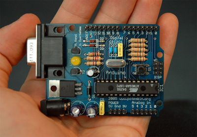
By Nicholas Zambetti CC BY-SA 3.0
But we all know that progress in the world of electronic components has not stood still. Surface-mount components have a history going back to the 1960s, and started to appear in consumer equipment from the end of the 1980s. More components per square inch, smaller, cheaper devices. Nowadays they are ubiquitous, and increasingly these new components are not offered in through-hole versions. Not a problem if your experiments are limited to the 741 and the 555, but something that rather cramps your style if your tastes extend to novel sensors for a microcontroller, or RF work.
This development has elicited a range of reactions. Many people have embraced the newer medium with pleasure, and the Hackaday.io project pages are full of really clever SMD projects as a result. But a significant number have not been able to make the jump to SMD, maybe they are put off by the smaller size of SMD components, the special tools they might require, or even the new skills they’d have to learn. When you sell a kit with SMD components these are the reactions you will hear from people who like the kit but wish it was available in through-hole, so this article is for them. To demystify working with SMDs, and to demonstrate that SMD work should be within the grasp of almost anyone who can wield a soldering iron.
But They’re So Tiny!
It’s likely to be the first reaction from a lifelong through-hole solderer. SMD parts are often very small indeed, and even those with larger packages can have leads that seem as numerous and thin as the hairs on a cat when seen with the rabbit-in-the-headlights panic of the uninitiated.
But it is important to take a step back and understand that not all SMDs are created equal. Some of them are grain-of-sand tiny and only hand-solderable by those with God-like powers, but plenty of devices are available in SMD packages large enough for mere mortals.
So don’t worry when you look at a board covered with grain-of-dust-sized components. Very few people could attempt that level of construction, your scribe certainly can’t. (We await commenters claiming to routinely hand-solder thousand-pin BGAs and 01005 chip components with anticipation, however such claims are useless without proof.)
Instead, concentrate on the SMD packages you can handle. SMD chip component packages are refered to by a number that relates to their dimension. Confusingly there are both metric and imperial versions of the scheme, but the format is the same: length followed by width.
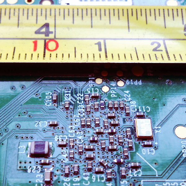
Consider the picture above with the PCB and the tape measure, it’s the underside of a Raspberry Pi model B+, and will have been assembled by a robotic pick-and-place machine. The majority of the components are very tiny indeed, but you will notice L3 as the black component towards the bottom left that looks huge compared to its neighbours. That package is a “1008”, 0.1 inches long by 0.08 inches wide. It’s still tiny, but imagine picking it up with a pair of tweezers under a magnifying glass. Not so bad, is it. You’ve probably handled plenty of things in that size range before, do SMD parts seem so scary now? The larger components – 0805, 1008, and 1206 – are surprisingly within the grasp of the average maker.
But I need all sorts of special tools!
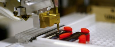
In a commercial environment an SMD device will be assembled by machine. Glue or solder paste will be printed in the relevant parts of the board, and a robotic pick-and-place machine will retrieve components from their tape packaging and automatically place them in their correct orientations. The board will then be soldered all-at once, either in a reflow oven or by a wave soldering machine.
If you’re new to SMDs you are unlikely to have any of this kit just lying around on your bench. There are self-built pick-and-place machines and a host of self-built reflow ovens, but it’s safe to say they’re still quite an advanced thing to have.
You’ll also see all manner of commercial kit aimed at the bench-top SMD constructor. Hot air soldering stations or SMD bits for conventional irons, all of which are very useful but come with a hefty price tag.
The good news is that you don’t need any of these special tools to dip your toe into the SMD water. You almost certainly already have everything you need, and if you don’t then very little of what you lack is specifically for SMD work. If you have the following items then you are good to go:
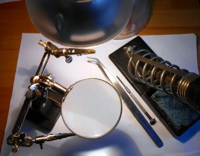
A good light source. Even the larger SMDs are still pretty small. Plenty of light ensures you will be able to see them clearly. A good downward pointing desk lamp should suffice. A clear high-contrast surface. Because SMDs can be difficult to see, it helps if they are manipulated over a bright white surface. A fresh sheet of white printer paper on a desk makes a suitable working area. Good hands-free magnification. Unless you are fortunate enough to have amazing eyesight, you will need a decent magnifier to work with surface-mount components. The “Helping hands” type on a stand are suitable. A very small flat-blade screwdriver. You will need this to hold surface-mount components down while you solder them. A good-quality set of precision metal tweezers. You will need these for picking up, manipulating, and turning over surface-mount devices. A fine-tipped soldering iron. If you have a standard fine tipped iron suitable for use with conventional 0.1” pitch through-hole components then you should be well-equipped.
That said there is one special tool that might be worth your consideration. Holding an SMD device while soldering it can sometimes seem like a task that needs three hands, so one or two tools can be found to help. Fortunately this is something you can build yourself. Take a look at the SMD Beak, a weighted arm for example, or your scribe’s spring clamp third hand.
I’m sorry, this is just beyond my soldering skill level
It is easy to imagine when you are looking at an SMD integrated circuit that its pins are just too small and too close together, you couldn’t possibly solder them by hand. The answer is that of course you can, you simply need to view how you solder them in a different way.
With a through-hole IC you solder each 0.1″ pitch pin individually. It is something of a disaster if you manage to put a solder bridge between two pins, and you race for your desolder pump or braid.
With a surface-mount IC by comparison there is little chance that you as a mere mortal could solder each pin individually, so you don’t even try. Instead you solder an entire row at once with an excess of solder, and remove the resulting huge solder bridge with desolder braid to leave a very tidy and professional-looking job. Surface tension and plenty of flux are your friends, and there is very little soldering skill required that you do not already have if you are an experienced through-hole solderer.
If you can hold it down onto the board and see it clearly with your magnifier if necessary, then it doesn’t matter what the component is, you can solder it. Give it a try, you’ll surprise yourself!
What next?
So we hope we’ve convinced you as an SMD doubter, that you have the ability to work with SMDs yourself. What next?
Start by reading up on the subject. Your favourite search engine should deliver, tutorials can be found from Sparkfun, from Adafruit, or from Instructables among many others. And look for videos, YouTube has a huge number of SMD soldering guides.
But there is no substitute for practice. Find a scrap board populated with reasonably-sized surface-mount components, and have a go at reworking it. Desoldering its components may be a bit difficult, but you should easily be able to rework the solder joints. Slather an integrated circuit’s pins with flux, and try running a blob of molten solder along them, then removing the excess with desolder braid. The great thing about a scrap board is that it doesn’t matter if you damage it, so you can practice these techniques to your heart’s content until you are satisfied with your new-found skill.
So you’re ready to move forward, and make your first SMD project. Well done! What you do next is up to you. Design your own circuit and get a PCB made, buy a kit, or find an SMD project you like on Hackaday.io with downloadable PCB files and order your own.
Whatever you do, be happy that you’ve conquered your SMD fears, and resolve to be first in the queue to try any new technology in the future!


https://hackaday.io/project/6580-smd-soldering-made-easy/log/33261-smd-soldering-new-and-improved
Enough said :p
I always impressed when I see QFN done with an iron rather than hot air.
Soldering a QFN with the “drag solder” method with a normal soldering iron and wire solder:
http://youtu.be/Ch4qOKsFZCU
Timelapse building a batch of SMD boards with a normal soldering iron and wire solder:
http://youtu.be/oeEOoQKwzgA
Enjoy. :)
Not all QFNs have leads which extend to the package edge that can be touched with an iron.
So long as the pad extends to where you can reach it, and it isn’t covered with solder resist, you don’t need to touch the lead.
Good luck not making a cold solder joint in that case.
Yeah, I had my doubts too. But with the right amount of solder paste and of flux, you just try it anyway. And the majority of the time, it works. Flux, wetting, and surface tension are wonderful things.
Oh, lead (Pb) is a wonderful thing too. Don’t mess around with that lead-free solder unless you’re under legal obligation to do so. Otherwise you deserve any problems you get, especially when using non-optimal soldering techniques.
@[Chris C.]
I once saw RoHS (lead free) car battery post connectors the ones that you tighten onto the lead battery posts.
This isn’t a “just try it” thing. There’s no way it can work reliably with wire solder. Think about it. If you heat the pad and flow solder onto it, if the solder goes *under* the chip, there’s no contact between the solder contact point on the chip and the pad. So there’s no heat flow. So the joint is cold.
If there *is* contact between the chip and the pad, then there’s no way for the solder to flow under the chip, because the edge of the chip isn’t connected to the contact point.
*Most* QFNs have contacts that extend to the edge of the chip, as that’s the JEDEC standard. But not all of them do. And the ones that don’t really require solder paste and hot air.
Nice video!
You mention diluting the flux with alcohol. What flux and what type of alcohol did you use?
You can even desolder QFN with normal iron.
“We await commenters claiming to routinely hand-solder thousand-pin BGAs”
What does “hand-solder” mean? Anyone can do high-pin count BGAs pretty easily with StencilQuik and a reflow oven. Yeah, StencilQuik adds a per-unit cost of like $10-20, but that’s a small modifier on the cost of a thousand-pin BGA.
01005 components, though, you’re on your own.
At the HaD conference last fall in SF, a German guy (sorry, don’t recall his name) did a quick presentation on assembling BGA parts at home. The trick was to not add any solder. Instead, just coat the area where the BGA is supposed to go with flux, position it as carefully as you can, and then cook the board in your favorite reflow oven / hot plate.
The point is, the proper amount of solder is already on the part in the form of the solder balls it comes with. You just need to let it flow onto the pads. The flux and surface tension does the rest.
I haven’t tried it, but he made it sound pretty straightforward.
I’ve reworked some DDR that way (0.8mm), but if you are doing a surface mount board you should be using a stencil anyway. The better you control the amount of flux, the better your reproducability, and having a stencil putting down paste lets you do that very accurately.
Yeah, StencilQuick just allows for perfect alignment by feel, so you don’t have to worry. It’s just a precision cut polyimide adhesive.
Er… humour alert.
On a serious note, WRT placing BGAs by hand for reflowing, by my observation of others doing it they find it very difficult to get them aligned correctly & thus have a significant failure rate.
Right! Because you didn’t notice the important part in my post. StencilQuik.
If you don’t want to click the link to see, they’re polyimide adhesives with the BGA pattern cut out. Yes, you can add solder paste to them, and that certainly helps, but the *most important thing* that it lets you do is align by *feel*. You align the StencilQuik adhesive onto the board, which is easy to get close to perfect – if you screw up, you can lift it and try again (and if you really screw up, well, $10 is often cheaper than the BGA part).
Then you put solder paste on, and then you put the BGA part on, and you can *feel* it drop into the holes for the balls.
If the $10/per cost of the StencilQuik turns you off, there’s a DIY example here.
To be honest the other thing I’ve been curious about is whether or not you could mill a small metal frame the size of the BGA, and put mounting holes around the board. Then you attach the frame, drop the BGA in, reflow it, and remove the frame. You’re trying to align things to a fraction of 1 mm. It shouldn’t be that difficult.
on a proper board with soldermask you can also feel it. Not as good, but still noticable.
Yeah, the StencilQuick basically acts to thicken the soldermask by a lot: normal LPI mask is like, 2 mil, and the StencilQuick adds about 4-8 mil on top of that, giving you around 6-10 mil total. BGAs balls are normally ~16 mil height, so you can see that the ~6 mil Stencil Quick means it’s half the ball height, which makes a *really* easy to notice the difference.You really can’t screw it up.
why would you want to notice anything? this is what flux and surface tension is for, chip moves to proper place on its own
global position is nice as surface tension would not fix every alignement error ;)
“You are a spammer, hacker or an otherwise bad person.”
— http://www.solder.net/products/stencilquik/
I don’t like the giant solder blob / solder braid removal technique. It’s very messy and runs the risk of overheating the part or damaging small pins.
The most important tip for SMT soldering is FLUX FLUX FLUX FLUX FLUX. Have bottles of liquid flux, tubes of gel flux, flux pens, plenty of isopropyl for thinning it out as needed, dispenser syringes and brushes and bottles with dispenser needles.
The second most important tip for SMT soldering is the tip of your iron. Clean, bright, plating intact, and not too small…a fairly large hoof or bevel tip will work great.
The third most important tip is to go on YouTube and search for “drag soldering” and hide your solder braid until you learn this technique.
Yea I just started doing surface mount and it’s all about flux. I use a flux pen and a regular crap iron and it works. I was surprised I was able to do it as I pretty much suck at regular soldering.
THIS! It is very easy to solder even very fine pitch parts with good quality flux and a decent iron. I use drag soldering all the time! I cringe every time somebody mentions solder wick or breaks it out to work on something because 90% of the time you will end up lifting traces and pads off the PCB, and possibly ripping the pins off your part!
I cant stress enough the difference a good set of tweezers makes! Break down and spend a bit of money on a good set and you will not regret it.
I have soldered 0201 parts pretty regularly at a past job, and the tweezers made the difference. You need a microscope for most of the work, but it is doable! Anything down to about 0402 is pretty easy with a desk mounted magnifier, but anything smaller and you really do need a microscope to even be able to inspect your joints.
Absolutely, the solder sometimes cools on the edge of the wick and bonds to a pin. When you lift away the wick….ooops.
That $25 chip just became an expensive piece of trash! Time to break out the magnet wire, assuming there is enough metal left to try and rig it up… (Don’t ask)
Sorry, don’t really understand the concern – this has never happened to me. One drags away the wick and the soldering iron together, the wick is “molten” at all times…
That’s what you’re supposed to do, but the one time you don’t do it is when you accidentally rip pads off your PCB. It’s a great mistake-fixer but I wouldn’t use solder wick as a normal and expected part of the soldering process, something you use on every pad.
I am try to avoid at individual parts smaller than 0402 as they get much harder to handle. I like resistor arrays as they have the best of both worlds – bigger than their singles and more space saving. e.g. 0302 has two 0201 resistors and yet for handling it is almost like 0402 and you have one less part to place.
The problem is that there’s more reason than just space saving to go to smaller parts.
An 0402 cap is simply flat out a better cap than an 0603 cap, for lots of cases. It has about 30% less parasitic inductance, because, well, it’s smaller. Which means that 0402 cap *stays* a cap to about 40% higher frequency than an 0603 does, at equivalent capacitance.
And unfortunately you can’t pull the ‘capacitor array’ trick there, because the *distance* to the thing you’re trying to have a capacitor on is what causes the parasitic inductance. So the caps have to be as close as possible. Which means tinier = better.
I really, really wanted to avoid 0201 caps as long as I could, but when you’re trying to run things at 500+ MHz, that extra decoupling can really help.
With physically small capacitors you have be careful with DC bias, with 0402 size caps values above 100nF start loosing a lot of capacitance with just a few volts applied to it. Most of the time I’ll need a 0805 cap if I want something close to 1uF at 5V.
That’s the reason why I didn’t say cap array.
There are only a few cases where you happen to get 2 close pins to take advantage of the array. Any time you go beyond a few mils of breakout tracks just to connect to a cap, you might as well forget about the cap and better off dropping vias directly to the power/ground planes directly and connect caps to the power/ground plane. Don’t forget that the power/ground planes act as a very low inductance high frequency cap.
Cap arrays can still help for decoupling – you flip the power and ground connections on one of the caps so that the current flow is reverse and some of the via and parasitic inductances get canceled out. There are cap arrays (e.g. AVX Interdigitated Capacitors) specifically designed like this for very high frequency decoupling.
Flux is the most important part. And proper solder that has lead. There is reason, why 40 years old TV will still work, while models from 2000s die of old age…
The smallest components I soldered were 0402s without magnifying glass or any other optical aid. I’m near-sighted, so it was a bit easier for me, but to check if the components were soldered properly I took photos with macro mode of my Dimage Z5. I messed up once soldering TQFP-100 with cheap Chinese flux. There were more bridges than in Venice. Good flux and a concave soldering tip fixed the problem…
Can people recommend some tweezers? A link to a global site like Aliexpress or RS/Mouser/Farnell etc would be great!
I’ve found a few different suggestions googleing, but no consensus.
It’s difficult to determine ‘good’ just looking on the web and there’s so much choice on tip shape!
I like those bent ones as they don’t block off my view. I like the Prideline bent tweezer near the lower right corner.
http://ep.yimg.com/ay/yhst-86144623803941/prideline-all-purpose-tweezer-kit-economical-3.gif
I got a couple from China as backup replacement. Haven’t used them yet.
I use the ESD bent ones from Adafruit. The sparkfun ones are too stiff.
Xcelite makes nice tweezers, I prefer the XSST7V for smaller stuff and the XHT-678 for bigger stuff. Amazon has decent prices or fry’s carries them on the shelf.
Hemostats can also be helpful sometimes, haven’t found a quality brand for those yet.
I have bought a few tweezers from aliexpress/ebay. First one was actually decent, I still use it. Then I splurged on 6 more for some reason, and they were so crappy I should just throw them away. I say buy a known brand instead, or from a reputable dealer anyway.
I find that after 20 years or so, my solder braid no longer sucks. B^)
Maybe it has oxidized…
I suppose the SMT flux I bought 15 years ago has probably crystalized in its container.
Put some flux on it?
Most of the time you don’t end up with a giant blob, the point I was making was that it’s not the end of the world if you do as a novice SMD solderer.
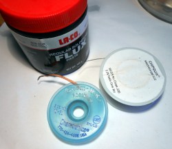
And yes, flux. And more flux. Hence the picture of the big tub of flux :)
I use bog sandard non acidic flux paste BTW, the type sold for plumbing. Works just as well as expensive SMD flux, cleans off easily with methylated spirits.
I suppose a non-acidic plumbing flux would work, but it seems the majority of plumbing fluxes are very acidic. Flux designed for electronics is so cheap, I wouldn’t risk telling beginners to go anywhere near anything that said “plumbing” on it.
Of course drag soldering is the way to go. But especially at the last pins some excess solder can very easily collect. And in this case some wick can be helpfull to remove this fast and controlled. And yes: Using enough good flux is the “beginning and end” to this.
Early on I managed to solder down onto a board that enabled one to use surface mount parts on breadboards, a DS2423 device, by hand using my regular iron. The part survived. QED
It just so happens that my project is aimed at providing a cheap entry point for soldering gear. Using high quality tips from Weller but cutting away the expense of the station.
https://hackaday.io/project/10140-soldering-pen
or you can buy this for less than weak weller tip
http://www.ebay.com/itm/New-Soldering-Iron-Temperature-Adjustable-12V-24V-72W-T12-Tip-Heating-Core-/262227023163
Which flux do you recommend? Are the “no clean” versions useful? What do I need to consider when choosing flux?
What you are looking for in flux is to have flux. Yeah, really. Lots of flux.
OK, there are preferences (I most regularly use Kester RA flux in a pen) but what matters is that you use it.
Importantly, flux can be corrosive and may become conductive, so it should be cleaned. If your board will be presented / visible, you will not want to use a no-clean as they harden and are very difficult to remove (they don’t require cleaning – thus “no-clean”). If it will be for a finished product without a PCB cleaning step then no-clean is fine. For prototyping it’s up to you but I usually clean my boards and thus use an RA flux.
Liquid no clean is a no no! It has horrible noxious fumes, and leaves hard to clean residues. I like the Water soluble kind, because it is easy super to wash off with a little hot water, an old toothbrush, and some ipa if needed. Kester 2235 works really well, and you can buy a gallon which will last you forever for a fair price. RA is a good option too, very flexible and works for just about anything, though it leaves a gooey residue usually.
Seems like a waste of good beer.
LOL. I see what you did there! Touche! Well its not a waste if you enjoy the ‘IPA’ while you clean, though you should really make sure it is the right ‘IPA’, or you could go blind!
IPA (as Isopropyl alcohol) does not make you blind, that would be methanol. AFAIK IPA has about the same toxicity level as Ethanol (the stuff most of us drink sometimes in alcoholic beverages). Which does of course not mean you should drink it, it is said to be no fun in comparison to “normal alcohol”.
Kester #2331-ZX Flux Pen. Fantastic, especially with lead-free solders. Also, for DIY, do yourself a favor and use regular 60/40 solder.
Lots of light and a glasses or head mount magnifier for good stereo vision. The magnifying glass is a PITA.
Run your iron hot. Flux pen the pads. Hold the part down with the pointy curved forceps and touch the whetted iron to one pin or side. Or tin the pads first, hit them with the flux pen again and the pin will settle into the melted solder very quickly, which is a good way to avoid too much solder (this works bets for me). I never need the solder wick unless cleaning up after a beginner on the re-work line in China.
I have a product that needs to have five 0408 resistors moved for one customer who buys 20 to 50 at a time. It takes about 45 seconds total under a stereo microscope.
Thinking about it, we use a brass sponge constantly to clean the tip and never “tin” them. A brass sponge in a weighty pot is another “must have” to work fast and clean. Also, hitting the sponge then touching a pin with too much solder will often pull off enough to not need any wick. Touch it with the flux pen first and you get a good looking joint.
The same brass sponge will get gooey stuff and fibers and other gunk off your forceps as well, and very quickly.
Currently using Kester #985M “low-solids, no-clean”. Works great. I don’t notice any noxious fumes. It leaves so little residue that the only time I’ve cleaned is sometimes after board RE-work, and even that isn’t truly necessary, just me being obsessive. It’s easily cleaned with IPA (IsoPropyl Alcohol). Used with an iron running at 600°F and standard lead multicore solder. Sometimes with solder paste, which is kept in the fridge but well past expiration, and has been reconstituted a bit with 91% IPA.
I admit I’m still a bit intimidated by SMD. My eyes aren’t good, my hands aren’t steady, I have to work slower, and still end up populating the carpet with a significant fraction of the 0402/0603 parts I use. For that reason, I still use lots of through-hole parts. But when SMD is necessary or clearly superior, I use it without hesitation. I’ve had no issue making reliable solder connections on the first try, and have damaged no components with excessive heat (except for one very tiny push-button).
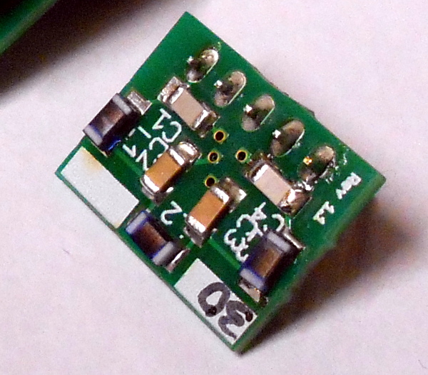
The flux in the picture is sold for plumbing here in the UK. It’s non-acidic paste, I apply it in liberal quantities with a cotton bud. After soldering my board is covered in flux, so it’s hardly no-clean, but a few seconds with a toothbrush and some methylated spirit sorts that out. The little filter PCB pictured was done that way.
The important thing IMHO isn’t what flux you use, but how much you use. Use a lot.
A few suggestions.
A good magnifier with a built in light source, a separate light and a separate magnifier with a different focal are what I have (that’s three items). This helps remove shadows from large pieces, lets you use one or the other magnifier depending on size or how tired you are or even double up on lenses and lights. Most people should already have a good light and the third hand magnifier so getting a magnifier/light combo shouldn’t be too much of a leap.
Instead of a flat screw driver, I use an X-acto knife with the #11 blade (careful with that point). With a little practice, you can get quite adept at applying solder paste, flux (I use a liquid I make myself), scooping parts up, cutting traces, holding parts down while soldering (use the back side of the blade). I don’t feel bad if the soldering iron damages the blade or if it breaks, I just toss it and replace it. I used to use, and still have my tweezers somewhere, for picking and placing parts but I got fed up with losing so many resisters and caps so I just dip the blade in a smidge of flux or paster and use it to grab the part like a sticky bun. Larger parts just get scooped up since I’m too lazy to switch to tweezers I can’t find anyways. I picked up the idea when I read about Chinese manufacturers using chopped and mushed chopsticks to pick up and place SMD components by hand. Did that for a while but liked the blade much better. Remember there are two sides to the blade, take advantage of both sides. Look at other X-acto blade shapes if the #11 doesn’t fit your style.
Buy a stereo microscope if you’re going to be doing any significant amount of SMD work. There are some cheap Chinese ones available on eBay which will work OK. Something like this: http://www.ebay.com/itm/AmScope-10X-20X-LED-Binocular-Stereo-Microscope-Boom-Arm-with-Gooseneck-Light-/400429192095?hash=item5d3b70939f:g:Pw4AAOSwbdpWYnDh
would work fine.
Get the finest tip soldering iron you can find. We use Pace, with the plug-in tips. They are NOT cheap, but they heat instantly.
I want a decent stereo microscope for my workbench, and it will be very useful for removing metal or wood splinters from my fingers (obtained in the woodshop).
A decent stereo microscope with a nice long (few inches) working length has paid off here in many areas, yes, including pulling wood and metal splinters, as well as making smd work almost too easy. Do it! I have surplus ones from edmund optical and B&L and the former is actually better (and a lot newer). Takes awhile to adjust to the bent optical path – eye hand coordination messes you up at first (and without one afterwards for awhile). Worth it. Variable magnification – priceless. I use paper background and a cheap halogen gooseneck desk lamp with a floodlamp.
Do it! Worth it for the splinters, and makes SMD work almost too easy. Most have a decent working focus length – 3″ or so. Paper background, halogen gooseneck desk light with a floodlight, worth it. Bent sharp-tip tweezers are dirt cheap at MPJA when they have them. Kester 952 flux is what I use (dilute with IPA if needed), and drag solder, once in awhile needing braid, but not always. If you’re laying out your own boards, I do the reverse of normal – I make the pads about 1-2 mils narrower than the pins, ensuring any bridges aren’t at board level, but up on the pins. Saves a lot of hassle removing any bridging. If you do it a lot, the expensive MetCal irons are actually worth it – I wouldn’t have believed that before I had one (think you nice customer for buying me something I’d never have shelled out for myself).
Agreed. But probably beyond the nervous beginners this article is aimed at.
The cheap Chinese 10-20x stereo scopes are in the $100 to $200 range. You can probably build your own LED light. Anyone doing any significant amount of SMD work should have a stereo microscope. As soon as you use it, you will know it’s worth the money. I can’t recommend these strongly enough.
Also handy for removing splinters from your (or someone else’s) finger, fixing small jewelry, etc.
If you make small things, buy one. You will not regret it.
Even a cheap mono USB microscope is under $40 USD and most still give a decent image. For some of us position is a major factor and avoiding the hunched over posture of some regular magnifiers gives much more time at the bench. This is a nice basic description but try and avoid the mistakes of a former HAD writer who mocked a couple of readers, including me, who said they always used magnification when working on boards. He was one of your typical theoretical builders who could mount .01 mm without dragging or ever bridging. Glad to see most of that attitude purged by editorial staff.
My advice – go get really sharp metal tweezers. When talking about component placement issues, this is the solution that never lets me down. Plastic tweezers tend to melt and are hard to sharpen, so just get tweezers and a de-magnetizer. Actually, get 4-5 pairs. You can gift them, and if a pair gets lost, you have spares so you don’t search for one of the most important tools instead of making things =)
I’ve started from 1206 – resistors/caps in that shape are still much better than through-hole in terms of space they take and therefore make it easier to route the board. Then I moved to 0805 (still manually placing them) and it’s very easy even with a relatively huge soldering iron.
You have to manage your parts a little more too. I used to be able to lay out resistors and caps and ICs and everything, out of their packages and be fine if they happened to get jumbled because I could quickly sort them out via color code or numbers. Now, on a lot of parts the numbers have no meaning as to which part is which, nor are their color codes. Best to leave them in their package or a labeled tape than to dump everything you’re going to need on your bench. IC’s are still marked and easy to figure out at least. Also you’ll likely have to etch a board or have one fabbed. No more protoboard. Most “solutions” to this are expensive and or a pain to use.
Well, I still have a collection of through-hole parts, and I buy through-hole parts exclusively for prototyping. Also, there are simple breakout boards for all types of footprints you can use, and you can easily solder smaller parts to 2.54 headers or male-to-male prototyping wire ends if you need to prototype on, say, a SOT-23 FET.
My SMT soldering method of choice is a standard kitchen-grade hot plate. Turn the plate on, apply solder paste to the board however you like, place the components, then pop the whole board onto the hot plate for a few seconds and remove it once all the paste has melted. Gently place it on a flat surface (I use a ceramic plate) and wait for it to cool, et voila, all your SMT soldering is finished in one go!
Though, this only works for boards where all the SMT components are on the same side (and requires a hot plate *without* a magnetic stir function, unless you like watching your components slide around the board in a big metallic clump).
Yes, by far, the easiest way to SMD solder is to not do it. Sitting there with a soldering iron and tweezers, tacking soldering, tacking soldering, is so incredibly tedious.
Another vote for using an electric hot plate. We use them for building prototypes and even some light production work with boards that have only a few components, along with an inexpensive metal stencil.
“Fear is the path to the dark side. Fear leads to anger. Anger leads to hate. Hate leads to Fritzing.”
The only problem is finding SMD kits. They’re really hard to find.
Does anyone have any links?
I use “cryovials” to hold my SMD parts. Not my idea, ’twas a departed tech’s at a place I used to work. They come in little boxes with cardboard separators and you can write the value on the screw-on lids. Check biological supply places. One set ofr R’s and another for C’s Different boxes for different sizes (though I use almost exclusively 0603)
Just order a cut strip of 100 whenever you order parts from Digikey, and put the extras in a cryovial. You’ll have a complete kit in no time.
One source: https://www.emsdiasum.com/microscopy/products/cryofixation/cryo_vials_racks.aspx
Get the plastic type with screw caps. Different color caps for R and C
My Digikey order from last year have nice blue static dissipative zip loc bags for a lot of the parts including cut tape SMT passives, so I just keep them in there. I have shipping boxes just the right width and they are handy for storing the bags. :)
Digikey has just recently started shipping in resealable bags. YAY!
One can get large cut-tape resister/ceramic-capacitor books on ebay for around $20.
We usually standardize around:
0805 for 1% resisters / LEDs
0603 for ceramic capacitors
1206 for fuses / diodes / larger-value capacitors
These sizes are practical to handle with tweezers, and are very forgiving for toaster-oven re-flows at home.
Note, you want to reduce the variations in values if possible, as this will lower the cost of building anything both at home and the factory.
Alcohol based liquid flux with desoldering-braid is a must have, and we can easily drag solder 84 pin QFNs even with a dubious solder mask (if you left enough clearance during design). Cleaning off the flux after is a must if you used paste, or you will never be able to inspect the chip contact areas for microscopic solder ball contaminants. Admittedly I was sceptical initially, but it turns out a QFN often will have far fewer solder bridges than fine pitch leaded parts.
It may seem counter intuitive, but smaller parts like 0603 have larger relative surface tension forces that will pull the SMT parts into position. Also, when I was a student people often told us to avoid plated vias on ground pads or the paste would re-flow into the holes and not bond the chip correctly. However, it has been shown that usually only around 70% of the actual pad needs coverage with SAC305 based solders, even 5 plated spaced vias significantly improve cooling, and a QFN chip will be less likely to wander out of alignment during re-flow if too much paste is applied. If you ever want to troll EEs, then claim its recommended practice for all reflow jobs. ;-)
I like seeing effective methods that avoid using death-in-can solvents around people. Note, most RoHS parts will rot in moisture, and unlike plastics won’t dry out easily. One should use a desiccant box with aluminium foil bags to extend the 2 year shelf life. Even excessive flux won’t really help the pad oxidation problem in some cases, but most re-flow adhesion problems I find are caused by oxide/crud or paste quality.
Also, if you only need 1 board than make 3… as most boards have a re-flow time characteristic one will need to adjust.
Beg the company for sample kit (perhaps a long shot if your not a company but maybe a engineering student). Digikey has kits,
I have to disagree with the part that says home reflow is an “advanced” skill. It’s really easy compared to hand soldering of SMD parts. The hardest part of it is obtaining a reflow oven, but even that’s not hard – most entry level hobbyists just convert a toaster oven. I sell a conversion kit of my own on Tindie, which makes it as easy as it’s going to get.
Once you have an oven, the rest is just using tweezers to place the components. I use 0805 as my standard size and it works just fine and the parts are plentiful. As I’ve gotten more experienced I’ve done TQFP packages and QFN on occasion. But my first project used nothing smaller than SOIC and 0805.
At this point, I’d say that hand PnP and reflow is actually faster than through-hole assembly. After all, all of the soldering is done all at once and there are no leads to clip. One board I make regularly has a mix of SMD and TH because it deals with high voltages. I estimate it takes a third more time to do the same number of TH parts as SMD in that case (YMMV). All it took was gaining experience and familiarity.
The last thing I’ll say is that the first time I did it, I thought it was going to be a disaster. It looked horrible when I was done with the placement. I almost threw it away but decided to run it through the oven anyway. The results were miraculous. As bad as it looked going in, when it came out it looked like it had been manufactured in Shenzhen. Use the (surface tension) force, Luke.
I even used a completely stock toaster oven for reflow on 100+ boards, the only modification was to set a kitchen timer nearby and manually control the profile :) 3 minutes on low, 2 minutes on high, shut off and let cool :)
It’s advanced if you are the timid beginner to SMD soldering this article is aimed at. But yes.
I *was* that timid beginner, and I’m trying to reassure those standing in the same place (with my 20-20 hindsight) that it’s easier than they think.
hot air and flux, thats all there is to it
SMD I say no to thee.
Please don’t make the mistake of repeating problematic SMD soldering tricks. They’re widely popular, but just aren’t correct.
First, let’s talk about component size. While large components might seem desirable at first, that is really not the case. With chip capacitors, for example, you want to go as small as possible; the larger cases are very prone to heat-related stress cracking especially when hand-soldering them incorrectly. Large versions of components are also rather expensive. I’ve found 0805 to be usable by pretty much everyone and 0603 to be just the right compromise between cost, size, availability and ease of assembly. 0402 is okay, but does require a bit more effort when placing.
The good light source I can agree with. It’s quite important.
Magnification is almost always *completely useless* for SMD soldering. It’s very important for inspection after soldering. It’s also important when doing bodge wires and can help with other forms of rework. Soldering works without magnification: you need to be able to manipulate both hands simultaneously in a precise manner, which requires direct visual feedback. You want to grab a component, place it, and solder it in one go. Using magnification is okay if you’re really having trouble seeing your component alignment, but other than that, it tends to make matters worse. Especially the recommended magnifier, as their optical quality is usually very poor, and they’re quite tiny, so they will constantly be in the way. For inspection after soldering, you want to have reasonable magnification, ideally a bit more than what you’d use for soldering.
Flat-blade screwdriver: Why? Don’t bother! You have tweezers! SMT components do not require force to be held down, so just use your tweezers. I’ve never understood the screwdriver; they’re hard to handle and you’ll be likely to end up scratching, nicking or otherwise damaging components.
Tweezers: Not sure if a set is required. Having multiple ones is nice, but you can do with one pair of tweezers as well. They have to be of reasonable quality, i.e. not bent metal junk. They don’t have to be expensive: I’ve had luck with Chinese(?) “Vetus” tweezers for a couple dollars, they were certainly worth their money. I do recommend Aven’s EZ-PIK series (I got mine from digikey), since they’re inexpensive and color-coded, which makes them stand out and thus easy to spot. It’s a matter of taste whether you want a straight or a bent tip, but if you’re serious, just get both variants. It’s not like 15 dollars or so for two reasonable tweezers is shockingly expensive. Over time, I’ve bought myself some ridiculously expensive high-quality tweezers. They are better, but not by a large amount.
Soldering iron. Oh well, where should I start? A fine tip will most likely cause lots of problems. SMD components are small, so you like to have maximum control. Fine tips are great for rework, because if you want to attach a wire to one single pin of a 0.5mm pitch package, you need to be able to heat just that pin. They do suck for soldering, because they don’t transfer a lot of heat. SMD soldering has to be done quickly, because components are definitely more delicate than their leaded brethren. Chisel tips are optimal. Pick one that’s slightly wider than the pads for your chip components and you’re done. I like to use 2mm or 2.4mm wide chisel tips (sorry, I’m not exactly sure at the moment) with my 0805s and 0603s. They can heat up a pad quickly and they’re not unwieldy enough to cause problems when components are packed tightly.
Soldering technique: PLEASE DO NOT USE THE FLOOD-AND-WICK APPROACH!!! This technique seems to be popular, but it’s amongst the worst things you can do. Here’s why: (i) It puts a lot of thermal stress on the component, (ii) it’s hard to do it properly, (iii) the quality of the resulting solder joints is substandard.
(i) If you solder all pins with a huge amount of molten solder, you’ll spend a lot of time heating them up. Then you heat them up again with your solder wick, which takes a long time. This puts a lot of thermal stress on the component. ICs do not like being soldered, so ideally, you’ll keep the thermal stress as low as possible. With this method, you’re heating the whole chip twice, each time extra long as well.
(ii) Solder wick needs to be warmed thoroughly. It’s hard to have this fully under control. If it gets stuck, you can easily damage a pad or lead of your component. It’s also next to impossible to precisely control the amount of solder sucked away. Which leads us to
(iii) the quality of the solder joints. There are lots of websites that talk about quality of solder joints of SMDs. Go look them up. IPC 610A provides more information, but that’s not important. What’s important: Pins should have a nice fillet behind them (heel fillet), to the front and to the sides. Solder on top of the pin or near the package of the component is not recommended. With the solder wick method, you first get a lot of solder on top of the pin and near the package. Then you suck solder away, which usually leaves next to no heel fillet remaining. Components soldered like that are rather prone to becoming unlodged by mechanical shock, because they’re just not attached properly to the PCB.
So, what should yo do instead? Drag soldering. There’s a lot of info online about how it works. It’s shockingly easy. I was anxious at first, but it worked perfectly fine the first time I tried it, on a 0.5mm pitch TQFP no less. You just have to use a decent amount of flux and try not to use too much solder. The pins and pads take up very small amounts of solder, so little solder is usually enough.
So, flux is missing on your list. Get the nicest no-clean gel flux you can get your hands on. Use it whenever you encounter problems, it definitely helps. Yes, nice flux is expensive and somewhat messy, but it’s absolutely worth it.
I prefer using a magnifier when soldering, even for through-hole. That said, I completely agree that the magnifier shown is total garbage. But a 5-inch fluorescent swing-arm magnifier doesn’t get in the way while you solder.
Until recently, I used a vintage Dazor articulated magnifier lamp, which would sit well above the work, and leave both hands free. Recently, I added an old Bausch & Lomb stereozoom microscope, and I’m loving it. Not as wide of a view as the magnifier, but the clarity is fantastic.
It may be a cheap-ass magnifier, but it does the job fine for my SMD work and doesn’t get in the way. :) I don’t use the crocodile clips though.
This article was written in response to some potential customers for my kit business being scared of SMD work. So it’s an eat your own dog food thing, I have to be able to assemble them using basic kit. It would be no use my selling them a kit I’ve only ever mde in a reflow oven.
I’m an engineer and do some of my SMD prototyping on regular 0,1″ perfboard. I also own a small 5cm^2 SMD oven using just 80W instead of most 1kW toaster oven builds.
For a single sided PCB:
– Put a (micro-)dollop of solder paste on each pad of the PCB,
– Use tweezers and a magnifier to place the components on their pads (don’t worry too much about alignment, capillarity will take care of it),
– Make sure SO is not home,
– Turn on fan to prevent suspicion from said SO,
– Place the PCB on the ceramic stove,
– Turn on stove, wait for solder to liquefy,
– Turn off stove, move PCB carefully to cold part of stove,
– Done,
– SO not the wiser.
Has anyone a recomendation if it is better to buy a sortiment of resistors / capacitors or to buy as you need?
If you have a specific design in mind, buy as you need plus a few extra (depending on your confidence level). If you are prototyping and aren’t sure, get an assortment of passives. No point in getting too many extra ICs unless you use a particular thing (buffer, transistor, etc) in a lot of designs.
For example, you could get this: https://www.adafruit.com/products/442 and stock up on a good assortment of 0603 parts.
They sell resistors/capacitors assorted values cut tapes on Aliexpress. You are looking at $2.08 and $3.82 for 36 values x 20 of 0603 resistors/caps. Even for practicing soldering, that is a reasonable deal. I don’t know what size you want, but 0603 is a good size.
http://www.aliexpress.com/store/group/Electronic-component-kit/506373_500791312.html This is one store I have shopped half a dozen times.
Depends on your goals and other factors. I purchased big SMD resistor and capacitor assortments from overseas on Ebay, which cost about $20 for both. Don’t waste money on more expensive assortments with included fancy organizers, unless those organizers can be expanded. Else you’ll have to use two organizations systems for additional values you want to stock, which gets confusing. Or consolidate under a single system, in which case the original organizer becomes wasted.
Virtually every project still requires me to place an order for something I don’t have, so the assortments don’t help much there. But I’ve miscounted the number of passive components in orders. Used more than I thought I needed, or lost more than I expected to the carpet. Found out I needed to alter a value. In all these cases, having the assortments saved me from paying dollars in shipping on cents of additional parts, as well as waiting for the shipment. The assortments have proved worth it for me.
A reel of 5000 0805 1% resistors is $13 from DigiKey. At that price, I don’t know why you’d buy cut tape unless you were literally going to ever build one of a thing, and if you’re contemplating learning to do SMD, it argues that you’re going to do that more than just the once.
I buy a reel of each value as I need a new one. That leads to logarithmic purchasing, sort of. :) There are a lot of applications where you simply need to get within an order of magnitude of a value – pull-up resistors for example. So start with the decade values – 100Ω, 1kΩ, 10kΩ, 100kΩ, 1MΩ. For 5v LEDs, you usually want a 330Ω series resistor. For 3.3v, it’s 150Ω. I’ve bought about a dozen values so far, but I’ve done a lot of projects.
I have run out of one reel so far – 0.1µF 0805 cap. That’s my standard IC bypass cap.
And if you think a full reel of every resistor value is too much, for small-scale users doing hand assembly, ordering 1000x on cut tape is a nice number to order to keep some in stock. A 1000x bag only costs a few dollars and takes up less space than a full reel.
I have been building electronics as a hobby for 50 years so I no longer have great eyesight but SMD is doable even so. A very bright LED light (not halogen to keep the heat and UV low) is very important. Most of my work is one off and size is not critical so I use through-hole wherever possible with breakout boards for the ICs. I have built a fairly sophisticated reflow hotplate for SMD. I prefer a hotplate to an oven as my boards are sigle sided and the heat goes where it is needed not heating up large components as much. I use an infrared hotplate to minimize lag. The main problem is solder paste placement. Maybe the paste I have been using is not of sufficient quality but it tends to be viscous and not stick well to the pads. I am thinking of moving to using solder masks even for small quantities for that reason. For mounting individual components I have found that pretinning the pads, using solder wick to remove any excess and then using no-clean flux and a hot air gun to mount the component works OK. As I usually mount single ICs on thru-hole breakout boards this works well enough. I wouldn’t use this approach for BGA though as inspecition is impossible. I have found a cheap Chinese USB electronic microscope invaluable not for use during soldering but for post soldering joint inspection.
Any thoughts on a good way to apply solder paste by hand or a good paste to use would be most welcome.
I find a paste dispenser is invaluable. The paste will stick better if you go over the board with alcohol to clean it first. ENIG also helps (thank you, OSHPark). If you try and come at the board vertically, and try to make a “hershey kiss” shaped deposit on the pad, that’s best. For ICs, I just lay down a log across all the pads.
For QFN, however, a stencil is mandatory, and a vacuum placement tool is indispensable.
My first batch of home built boards used 0805 components. Applied solder paste using a syringe, and reflowed in a cheap oven. It is easily done at home. My latest boards require 0402, which is a bit harder to do. While I regularly do 0402 at work, I don’t like to do it at home because you want a good magnifier to inspect it. You could do it with a stencil, but rework later on would still be difficult.
I have done 0201, and only a handful of 01005, I wouldn’t recommend them. Hot air works best for parts that small. In any hand-rework it can help to have the board pre-heated, this will minimize chances to damage the board. I’ve even used a 500 watt halogen shop light to heat up boards.
A good soldering iron is a must, with good tips. You need the iron to have contact with the pad and the pin at the same time, hoof and chisel tips work well for this. For 2 pin components like resistors and caps you want to use two irons, one in each hand – it’s faster and the surface tension will align the part.
Through hole is slow as compared to SMD. I can solder a SMD device 10 times faster than a through hole. It takes a bit more practice, but is worth it.
Take a look at a pro. Sorry for the focus, it was an old Flip camera. That is an ARM11 6410 board several years ago getting a NAND upgrade.
https://www.youtube.com/watch?v=w-a2MluuURk
I remember the first time I tried SMD (with no flux) and things went into a large solderblobmess. Later on I ‘discovered’ flux and things went much much better. Nowadays when I’m really lazy I use solderpaste and hotair or oven. Got myself even a tool to cut stencils in notime.
Shameless plug alert :): at this very moment my learn how to solder kit is being kitted. What are the odds :) More info here: http://smdprutser.nl/project/learn-how-to-solder-kit/
It is a kit that will produce a highly variable resistor with a bit of precission (0-1MOHM in 1OHM steps) with 54 0805 resistors. All you need is a decent soldering iron and flux (or solderpaste and an oven but that is no fun :D)
You should run an article on where the different “Open Pick and place” projects are churning along. I remember Firepick, OpenPnP and LitePlacer. The last one is the only one actively shipping PnP machines.
What is your time worth?
I priced out DIY platforms for home use, and concluded even a Neoden 240 machine is more economical.
i.e. your opportunity cost rate would be below $1.50/hour to build something similar.
Fast food workers would laugh at you.
;-)
Most hobbyists wouldn’t benefit from a PnP machine. At the volume most hobbyists do, it’s going to be an order of magnitude faster to place the parts by hand than it will be to set up the machine to do it.
If you’re like me, and you have a Tindie store and make lots of the same thing, then that’s a different story. But even I haven’t gone there yet. Instead, for a few of my most popular products, I’ve outsourced the assembly. I’d still argue I’m probably ahead doing that than I would be acquiring my own PnP and then setting it up.
This is true. Really. ;) https://www.youtube.com/watch?v=96iJsdGkl44&index=3&list=RDEQa4HHkhwVg
Shameless plug, but if you want to hold a PCB stable while soldering SMD parts, try a Stickvise. You don’t have to buy one, although you won’t regret it – you can easily make it yourself from scraps if you have the tools and the time: https://hackaday.io/project/3287-stickvise-low-profile-soldering-vise/log/29431-scrapvise-and-other-stickvise-builds
Holy moley, that second image is crazy. What a rat’s nest by modern PCB standards.
It’s a VFO I picked up at a radio junk sale about 20 years ago. Probably early ’70s judging by the components. Very of its time. :)
Having been forced into soldering 0402 and some QFN part in a pinch, I’ve developed a few “Cheater’s” methods for these parts.
1) First thing I do is assume that anything I remove is toast, will be exposed to far too much heat; not reliable in the future.
2) With all small SMD passives (and plenty of ICs) I tin a single pad, then place the part while keeping the pad “wet”. You animal…
3) I have wire wrap wire on hand at all times that I will take a ~2″ length of and wrap 3/4 of around the soldering iron element. I then form the remainder into a pointy extended tip that I use to buffer the part from the “thermal inertia” of the soldering iron. Often this will let me apply some very fine solder to even 0201 in an extreme pinch.
4) Sometimes I solder a small length of 30 AWG to a pin as an indirect heat transfer path from the soldering iron. I just tin the lead of ~30 AWG, stick the part to it with a tiny amount of solder, then use the lead as a physical fixative as well as a way to transfer heat to the pin.
Side note: I am slightly myopic, and consequently I can resolve lots of detail with relatively close focal points. I mostly wear glasses but when I wore contacts to work I was unable to see as well close up, given that glasses can be taken off. Hence contacts can be an impediment to working with small parts. Get your mind out of the gutter
Personally, I don’t use a magnifying glass when soldering (the smallest I routinely do is 0402 on extra small pads). It’s in the way I think. For inspection, it’s great. But, the pro-tip here is flux, flux, flux and a good light source. Personally I use liquid flux from a syringe. Fluxpens are worthless, since you have to press them against the board. Soldering QFNs are no big problems, as long as the pads extend on the side (so you can drag solder them).
I actually do own some 01005 components, but I’ve never tried to solder them. I should do that some time, just to try it and see how horrible they are.
The worst project, solderwise, that I’ve worked with is my picosumo (1.25cm cube robot). The board is 1x1cm and has lots of 0402 (with extra small pads, since the standard in Eagle are huge). The board even has a bodge-wire, due to a design mistake.
Btw, murata has actually demoed capacitors smaller than 01005. They apparently made metric 0201 (link below), so don’t you complain that the SMDs are too small. It could be much worse!
http://www.murata.com/about/newsroom/news/product/capacitor/2012/0905
There is one advantage of using through-hole that I haven’t seen mentioned – if one _doesn’t_ order one’s PCBs manufactured professionally but uses some sort of rapid home-production method, routing rapidly becomes a problem as either everything is on the single layer you have or you need to muck around with through-riveting / soldering in pieces of wire / whatever. On the other hand, through hole gets you “free vias” at every pin – you can route from each pin on either side, and lining up the two sides at through-hole pad sizes is usually not particularly problematic with a bit of care.
Wow. I am doing NOT any of this.
I hate flux the environmentally exposed surface of flux absorbs moisture and becomes partially conductive and that in turn acts like a huge parasitic capacitor to the traces on the surface of the PCB so I use as little flux as possible. Also with modern packages these is very small separation between the bottom of the package (VQFN for example) and the surface of the PCB. Capillary action will such so much flux into that small cavity.
As a side note: I use some of the fluxes mentioned here to cold soldering / silver soldering / low temperature brazing or what ever it’s called where you are.
I also use 60/40 solder.
Rather than use more flux, I focus on surface preparation. I have spays / solutions that will remove oxidization and contamination.
I drag solder fine pitch parts and I always get left with a solder bridge between that last two pins. Sometimes I will use braid for this and sometimes I will angle the board and apply more solder (flux really) depending On what I think will expose the chip to the least heat.
Apart from that I can only add that I light box or any concentrated light helps a lot. I will try to get pic.
VQFN 100 0.5mm
Clear as a bell on a good light box light box (5600+ degrees kelvin).
https://cdn.hackaday.io/images/9345931458294540615.png
That’s a QFP not QFN (has external leads)
Bent leads on top right and bottom right cause shorts, especially the top one.
Without a proper side view it’s impossible to see if you have correct fillets on heel/toe of the lead. Surface finish of joints is also invisible.
As for flux causing issues later on… clean your board after soldering and you will never see any issues.
I make a lot off one-off stuff, and in that regards SMD isn’t very practical. I guess? You can’t just grab a strip board and get something put together. The need for custom PCB is higher, and that isn’t very practical, in my opinion.
I would like to be proven wrong though. Are there any good routes for one-off/prototyping circuits using SMD components?
For stripboard, give SMD resistors and capacitors a try. 1206 and even 0805 components can be hand-soldered directly to the strips, giving you a nice tight layout.
Generally speaking, SMD is awesome for one-offs if you can quickly spin up your own PCBs but hate all that drilling. I can probably whip up a PCB design and toner-transfer-etch it in the time it takes me to do the layout and point-to-point wiring on a stripboard.
That said, both the PCB layout and the home manufacture have learning curves that need to be climbed before it pays off. Stripboard and breakouts for SMD parts can let you get stuff done with less learning.
I guess the time for actually learning to make som PCBs is closing in. Probably not that hard, it is just a matter for actually getting the stuff I need to do it.
Sorry for the shameless plug, but I offer prototype boards for SMD. It accepts most common smd footprints like SOIC, 0805/0603 RCL, smd switches, 0805/0602 LED, etc. http://smdprutser.nl/project/breakable-smd-prototype-board/
I have lots of SMD parts lying around so most of the prototyping I do is SMD. It also doesn’t take much space so the wife doesn’t complain much :)
i think my biggest issue is sourcing parts. been using some tqfp microcontrollers for awhile now. problem is most of my inventory is salvage through hole parts. salvaging smd parts has been much less fruitful. most parts are not marked, so while its easy to figure out whats what (as far as passives go) is easy, determining value is less so. resistors usually have codes, and if they dont my multimeter helps. all the inductors and capacitors without codes now, are the bane of my smd experience. my cheap meters cant measure those. moving beyond passives, ive found it difficult to find data sheets on thins like diodes and transistors.
and the other thing that kind of holds me up is boards. many of my projects are on various proto boards. some have been rather nice having places to put various smd parts, but 9 times out of 10 i cant use the part i want with the board i have. i do make my own boards when i can. but again all my stock is wrong. the big thick double sided boards i have are overkill for surface work, and i am always broke. one of these days im gonna get some lighter single side stock and just use jumpers like most sane home etchers do.
I tried SMD for the first time a few years ago and NEVER went back. All I had then was a tweezer and my soldering iron. Now, I use tweezer, toothpick, soldering paste and electric skillet.
Like most tricky things, practise makes perfect… Anyone have any dead HDs/similar? Our kind sysads at work had a big pile I used to steal the controller boards from. Desolder some ICs, then put them back on again. Repeat 10 times. :-). Granted I date from a time where the boards had as many as three ICs, TSSOP flash, SDRAM and less BGA than now, but plenty of dead HDs are ancient too. :)
“We await commenters claiming to routinely hand-solder thousand-pin BGAs and 01005 chip components with anticipation, however such claims are useless without proof.”
How about reworking 0201 metric all day long? When just the BOM for one board is in the five figures you have no options but to learn.. In the end not so difficult with experience and good tools (stereo microscope e.g. Mantis is a must have).
Alas, no proof.. Damn NDA’s :(
I’ve learned to only solder smd with solder paste. It has saved me hours od headaches. A tube costs like $30, but I’ve had mine a year and I do a lot of soldering. Either have a stencil for multiple boards or use a needle syringe to put blobs on pads, the add parts. It has just the right amount of flux and solder and all you have to do is hit it with a sharp iron for 2sec.
When soldering with regular solder, get the very thin expensive stuff. Works great too.
Oh and I do 0603 this way, sometimes 0402.
This post couldn’t have come at a more opportune time. In passing the company owner asked if I had any micro soldering experience (not enuf to be confident) because a major loss of his business is shipping parts out to be fixed via micro soldering, so I told him I’d look into it. I’ve been practicing on some junk parts that use smd using a slightly more fine tip on my typical go to soldering iron and have had (not perfect) but promising results. This post has given me hope that I do in fact have the skill. Some of the replies have given me specific things and techniques to research to make the over all result better. Thank you Hack-A-Day stranger. If you have any haters (and you will) that come from this post, just know you at least have 1 complete success. That’s all matters! Take care bruh.
Thanks :)
I’m an old skool user. I like the thru hole. But, I do indeed have an open mind and want to keep up on the technology. Not totally scared of SMC, as I harvest quite a few of them for my projects. The hand soldering isn’t the issue I find. The thing I find really difficult is identifying these tiny things. Some of the larger are easy enough (Yellow caps, larger diodes), but majority of resistors, inductors, smaller caps. Well, good luck. Even with my home built SMC component tester, I can never (Read rarely) get the contacts good enough to test, and try to figure out what they are.
Anybody else have this issue ???
tester? identifying? recycling old parts? smd components are cheaper than sand
I use a DSLR camera which surprisingly is quite good for macro. I recently bought a Wi-Fi SD card for it so that I can download pics across the LAN without cabling the camera (USB) or remove the SD card.
It’s also on a tripod so I don’t have to take 5 of each picture so that I can pick one that came out (shaky hands).
For inspecting SMD soldering I use a light box as most of my protos are single sided.
Smart tweezers are essential for salvaging smd parts, they tell value and polarity. You need to exacto cut the traces and have a bit of wiggle room for cap values but it can be done. Cheap as sand doesn’t matter when the parts are two days and five dollars shipping away, it about convenience and philosophy, not price in most cases. Passives can be had for free with the heat and slap method and rarely suffer heat damage this way.
I think “Scared Of Surface Mount” is too vague to describe the choices I make for prototypes.
It’s more like I am scared of drilling holes. My most recent proto is single sided (zero wholes), has a couple of 74HCxx chips that have the legs bent out at right angles so that they can be soldered to the top of the board, several surface mount 0.1 pin headers for IDC that I made by removing straight pins and inserting right angle pins it also has a 0.8mm QFN44 CPLD (VQN44) as glue logic.
I do avoid very fine pitch chips for two reasons: 1) It hard to make tracks for them using toner transfer and 2) it’s harder to solder them without a solder mask. So I go to 0.8mm. I could probably do 0.5mm but I don’t want to try.
So it may be the case that I avoid holes. I don’t *avoid* SMD as I even surface mount non-SMD components. What I *do* avoid is holes lol. I need a cnc for holes.
Most non-SMD components can be surface mounted anyway.
“It’s more like I am scared of drilling holes. My most recent proto is single sided (zero wholes), has a couple of 74HCxx chips that have the legs bent out at right angles so that they can be soldered to the top of the board”
I do this too. Fold the pins of a DIP under, clip off the thin parts, and you’ve got a surface-mount DIP. Beats drilling.
But I’ll also double-side a layout when I need to, and then the holes are on your side.
I’ve been working with surface mount components ever since i left college and enjoy the challenge that it presents. I’ve created a website that focuses on the surface mount assembly process to help others with some of the many technical aspects – hope your readers find it useful – http://www.surfacemountprocess.com/
sphaaaammmm
I take that back; good website. :)