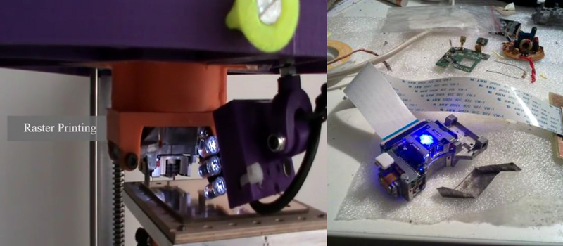
According to [diyouware], inside of every HD-DVD player is a gem of laser engineering with the designation of PHR-803T, and it’s just begging to be converted into a PCB exposer. Following along similar hacks which tore the laser diode out of Blu-ray players to expose PCBs, they wanted to use the whole PHR-803T unit without disassembling it, and to try to enable all of its unique features.
They envisioned something simple like a scanner for their machine. Just place the PCB on top of a glass sheet, close the lid, and click print. Unfortunately, moving the laser itself just caused too much vibration. So they switched to an inverted delta robot and named it TwinTeeth. In this design, the laser would stay still and the PCB would move.
What follows next is a seriously impressive journey in reverse engineering and design. The PHR-803T had no data sheet, but a ton of features. For example, it can autofocus, and has three different laser diodes. So many interesting problems were found and solved. For example, the halo from the laser caused the surrounding photoresist to cure. They solved it by adding a glass plate with a UV filtering film on it. Only the most focused point of the laser could punch through.
Another adventure was the autofocus. They wanted to autofocus on all four corners of the board. The PHR-803T was designed to read HD-DVDs so can focus a beam to far below 0.01 mm. They got autofocus working with the UV laser, but couldn’t use it on the PCB without curing the photoresist. So they put a piece of aluminum foil at a known level to start. Then they realized they could use the red or infrared diodes to focus instead. Now they can level the PCB in software, and focus the diode without curing the photoresist.
In the end they have an inverted-delta mini PCB factory. It can produce boards around the size of an Arduino shield with a resolution of 600 DPI. Their machine also has attachments for drilling and solder paste dispensing. Check out the video of it in action.


Very well done!
I am super excited about CNC exposing and I appreciate this post. Nice to see great hardware reverse engineering being done in the name of new design!
Nice work, but at only 600dpi we are talking about a complicated, fragile and slow machine that will achieve the same result as toner transfer and a much worse result than just printing out a transparency and exposing the board directly with UV light. What is exactly the advantage of doing this?
Also I wouldn’t want to use that hardware configuration for drilling – for that you need a rigid and really square frame, not a 3d printer. Otherwise the thin drill bits are going to break. A good drill stand would probably do a better service there.
I agree. Impressive work, but for a poor end result. In the video you can see the traces are iffy and the drill wanders off centre.
I feel like the problem is the delta robot, because the laser can do far, FAR above 600DPI. The joints on a delta need to be absurdly precise if you want very accurate motion on the actuator, since levers are a thing. A cartesian bot would require more expensive linear bearing components, but it could manage much better in terms of resolution.
In fact, if you watch carefully (at the 6min mark) you’ll see the PCB shifts as the drill starts drilling and it shifts back as the bit is retracted from the material.
A lot of the flex with the drill could be eliminated simply by leaving tiny etched-out centers in the drill holes. Both Eagle and Kicad will do that as a feature, and I do it with toner-transfer all the time. It makes the drill self-center a bit if there’s a little play in the system.
That’s brilliant.
I have a $50 Harbor Freight drill press. The spindle (think that’s the name) deflects when I start drilling. Enough to quickly snap tiny carbide PCB bits. But I figured out how to make it work. I used a string to tie a few pounds of weight to a non-rotating part of the spindle, arranging the string so it produces a sideways force on the spindle when the weight hung freely off the table. Anything with spring action is easy to move at first, then gets progressively harder. Pretensioned with a weight many times that generated when drilling, the spindle barely deflects at all; producing accurate holes without snapped bits.
Wouldn’t be surprised if a similar solution works for this delta bot. May be as easy as attaching a bungee cord between the platform and the frame while drilling.
And that’s why we came – for hack solutions!
Just pay a little more and buy a Proxxon mini drill press. Those things are totally rigid, never broke a bit with it.
Guess it depends on what the 600dpi really say about the system. I mean, if that machine can do exposure down to 0.05mm precision (25.4/600), it would truly be way beyond anything you can reach with toner transfer and transparent film UV exposure. From my personal experience, even if you tell your normal laser or inkjet printer to use 1200dpi, the end result is never good enough to etch 0.15mm traces reliably.
For the twinteeth, at least the Laser would have no problem to expose your board at that resolution, the only problem it has is the accuracy of the x-y-stage that is lacking because of too many cost savings implemented. I’m pretty shure that if you would throw more money into a precision guided backlash free x-y-design, it could compete with commercial pcb quality.
The problem is that then it would cost as much as a professional prototyping machine. That sort of precision mechanics is not cheap.
Toner transfer can do 0.2mm (8mil) traces no problem with a 600dpi printer (I am doing it quite regularly), if you do photolithography (aka expose a transparency), then 0.15mm is feasible with a 1200dpi printer.
Yeah, I was surprised to see the etched PCB – it’s easy to do better than that on a mini CNC mill with an engraving stylus. I would have expected to get _much_ better results with finely-focused laser exposure…
600 DPI is not “only”.
Send your PCB to a cheap chinese manufacturer, they do “6 mil”. They appreciate you staying “above 8mil” but officially they do 6 mil. 600DPI is 1.6 mil. Even if you’d be required “at least two pixels”, that would be about 3 mil: Twice as good as the cheap PCB manufacturers in china.
Imho, just being able to achieve what the cheap shops can do is “worth it”: You can prototype much faster. Two weeks ago I changed an optocoupler for one with a different footprint. Stupid mistake: The pinout of the optocoupler is unlogical (to me) and I wired it up the “logical” way. Wrong! So now we’re two weeks further before I have working PCBs…. That sort of stuff can be prevented by doing a “quick prototype” in your own office.
You cannot consider that every “dot” of that DPI can be a trace!
That “two pixels” wide trace would be pretty much unusable, because you will have a line of square pixels, not a reliably continuous electrical conductor. 600dpi is barely enough to make 8mil traces reliably and even with those you see the aliasing and sometimes some thin features get lost.
Also, every dot is not a square pixel, it is a round blob that must overlap the blobs around it.
This has been featured here before:
http://hackaday.com/2015/02/23/twinteeth-the-delta-bot-pcb-factory/
and even before that
http://hackaday.com/2014/02/03/laser-based-pcb-printer/
No vias, no soldermask, hazardous dust. Meh. I think I’ll just pay for a proper PCB.
amazingly developed project – well done for keeping on working on it!
Quick Idea:
wouldn’t it be great, to have a CD-Shaped PCB with laminated Photoresist, which can be Photoengraved using a normal CD-Writer and Lightscribe technology?
Size would be OK for small PCBs
Resolution would be high enough, but maybe the Resist will not be exposed dense enough.
https://en.wikipedia.org/wiki/LightScribe
https://de.wikipedia.org/wiki/LightScribe#/media/File:LightScribe-Spuren.jpg
What about using this for making custom ICs via the planarization method?
This could work for very simple circuits and Si is available in wafer form for not much coinage. Also using toothpaste + laser can etch silicon according to some articles i found.
You’re all missing the point of the video … this was a watch advertisement.