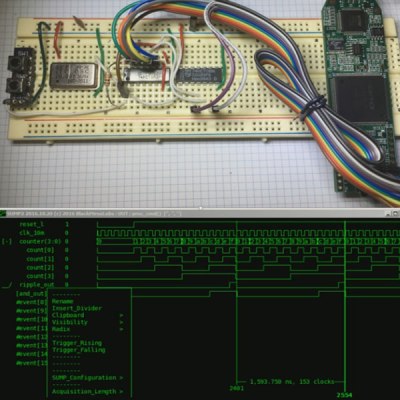
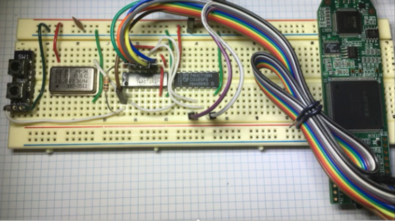
On my way to this year’s Hackaday SuperConference I saw an article on EE Times about someone taking the $22 Lattice iCEstick and turning it into a logic analyzer complete with a Python app to display the waveforms. This jumped out as pretty cool to me given that there really isn’t a ton of RAM on the stick, basically none that isn’t contained in the FPGA itself.
[Jenny List] has also written about the this application as created by [Kevin Hubbard] of Black Mesa Labs and [Al Williams] has a great set of posts about using this same $22 evaluation board doing ground up Verilog design using open source tools. Even if you don’t end up using the stick as a logic analyzer over the long haul, it’ll be very easy to find many other projects where you can recompile to invent a new purpose for it.
About the Stick
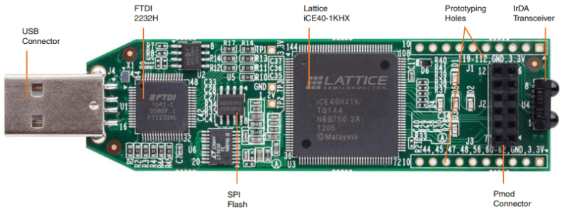
The Lattice iCEstick is a small FPGA evaluation PCB with only a little bit of support circuitry; basically just the FPGA, a clock, some SPI flash memory and a USB interface. There are also some connectors and pin pads as well as an IR transceiver to get signals on and off the assembly.
The FPGA itself is an iCE40HX1K with 160 logic blocks in it and up to 8 kilobytes of RAM, to me this sounds like a medium-small device, however since FPGA architectures differ I really can’t say for sure unless I wetre to load a couple of older designs I have used in the past for comparison.
About SUMP
I had been looking at the original SUMP.org analyzer for dropping onto one of my little custom FPGA boards I make when I am bored. I think of the logic analyzer application as a RAM pump (circular buffer controller) with a UART on one side and lots of I/O lines on the other. In general the amount of time desired to be captured at any particular clock frequency, translates directly to the amount of RAM needed. Protecting the FPGA from the harsh realities and in some cases the operating voltages present in the target system, is also important if using it for serious work.
SUMP2
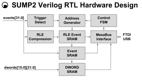
[Kevin] refers to his design as SUMP2 and for good reason as there is some departure from the original SUMP architecture. The SUMP2 utilizes a simple lossless compression scheme called Run Length Encoding (RLE) where instead of sending a large number of 0’s or 1’s in a row, it sends a bit value and how many times to repeat that value before the next transition to a different bit state. The SUMP2 design compresses the data not just for sending it to the controlling computer but also before storing it in the limited amount of RAM in the iCE40. Again this means that it isn’t necessarily the amount of time (or number of sample clocks) that determines how much data is stored but instead the number of transitions recorded.
RLE
Looking at the block diagram it can be seen that the architecture also supports non-RLE encoded data sampling as denoted by the signals named “dwords” at the bottom left.
There is a programmer available for free off of the Lattice website to program the iCEstick and the Bitfile can be downloaded from the Black Mesa Labs website.
To get more of a hands-on experience I recommend downloading the entire project and then download the free FPGA design software iCEcube2 from Lattice, though they do require that the user submit the MAC address of their computer to obtain the license key to run the software.
In the video I step through loading the project and all for the steps up to compiling the RTL code and programming the FPGA. That’s my way of saying I am not going to repeat all of the steps here.
The other piece is the Python GUI which consists of two modules, a server module named bd_server.py which camps on a TCP port and interfaces to the USB, and the core sump.py module which runs as a pygame application. Before running the app a couple of modules need to be loaded (this is all contained in the installation instructions), namely pyserial, and pygame. I used the following commands (I am not a Python person, you may have a more insightful or efficient l way):
“python -m pip install -U pip setuptools”
“python -m pip install -U pip pyserial”
“python -m pip install -U pip wheel”
“python -m pip install -U pip Pygame”
But wait, nothing is quite that simple, the instructions (and the video) walk the user through also setting VCP on the USB B port of the Lattice device driver. When and if you are successful you will be rewarded with the value for the virtual COM port.
The GUI
The next thing to do is to run the bd_server app from the Windows CMD prompt “start bd_server.py”. It may fail the first time but it leaves behind a configuration file “bd_server.ini” in which the settings for the COM port and can be edited. Changing “AUTO” to the proper COM port appears to be a common requirement. Running the app a second time resulted in a “5 by 5” message indicating that it was properly running.
Running the SUMP app itself “start sump.py” pops a window and the analyzer appears in all its green-tube-like glory (I changed mine to violet as seen below… or is it called purple?)
From here one is free to start analyzing and modifying if y’all have an interest to do so. For me, I found a line in sump.py and un-commented it so that the menu offered a direct way to make things bigger so my old eyes could actually see what I was looking at (turns out “home” and “end” always work for expanding the line height but I only know that from reading the code.
One note is that the FPGA used here is only 3.3V tolerant, [Kevin] has a public domain PCB up at OSHPark for converting to 5V.
Fini
If you have a serious need for a logic analyzer, use a serious analyzer, however if you want to spend a minimal amount of money and/or like open source stuff, check this out.


wanted to buy that icestick dev board this week, but Farnell didn’t have it on stock so bought a more expensive version. Then I wanted to install the icestick dev software, but the website had a 502 bug so I couldn’t get a serial.
So went with the icestorm open source instead. Have not used it yet, but already have more faith in it than the official stuff, given how things turned out.
Hopefully I can use Bill’s example on that dev board. Great that he’s doing this.
I got this one from Digikey (I gave the first one to someonein need) and I think Mouser probably stocks it as well.
When Al ran his posts on the Icestick, Mouser and Digikey both stocked out. Coincidence? It could be that ~300 Hackaday readers went out and bought them all off the shelves…
@mime: Icestorm on the 8k FPGA dev board is a fantastic setup. You will be able to do just about anything you want — both from a # pins and a # logic units perspective. I haven’t run Al’s tutorials on it, but I have every confidence that they’ll work. _And_ there are more LEDs onboard to make blink :). (You might have to change some of the pin definitions.)
The icestick is tiny in comparison at 1k logic units. But as the SUMP2 project demonstrates, that doesn’t make it worthless by a long shot.
For whatever reason, Lattice decided to build the iCEstick with the iCE40HX1K-TQ144 @ $4.41. The iCE40HX4K-TQ144 @ $5.37, or less than $1 more would have had 4x the capabilities. When I find an around-to-it, I would like to buy an extra iCEstick, de-solder the HX1K and solder an HX4K onto the board (same footprint ). Or maybe Lattice could just sell this as a product???
I bought an iCEBlink40-HX1K for almost double the price of the iceStick. I think in the end it was a better buy not only for the extra I/O pins you get, which will come in useful once I’ve gone past the starter projects.
It’s got 100 pins and 72 I/Os.
iCE40-HX1K-VQ100 100-pin VQFP (14 x 14 mm) 0.50 mm 72
http://www.clifford.at/icestorm/
thanks, I’ll consider the 8k board once I’ve exhausted the 1K I’ve got now in the iCEBlink40-HX1K
I’ve bought it on Aliexpress and I received it last week.
Just a small thing that cached my attention. In the video, at 14:10, when you are changing the COM port in the ini file from AUTO0 to COM19, you are actually editing the comment part of the line, not the actual setting.
I wish I had some knowledge about the topic to have a real discussion :) Thanks for the video and the post.
I made a 3D printable case for the iCEstick a while back, if anyone is interested…
http://www.thingiverse.com/thing:1862277
I meant to mention that! Thanks for the link.
If you have one of these sticks already then why not I suppose, otherwise the way to go is the Open Bench Logic Sniffer – exact same thing (FPGA / Sump / RLE), except sampling clock goes up to 200MHz, it has 24 Kb RAM and 16 or 32 inputs that are 5V tolerant right out of the gate, for $50. With a neat looking cross-platform Java client. All of it open. And it can simulate an ENTIRE HP 16550a if you really want it to, but it’s going to take some doing to get that to work. Frankly, it’s so well known it’s a bit disingenuous to talk about FPGA built-in RAM based LAs without mentioning it. Anyway, no relation, I’m just a fan (and a happy owner)…
Open Bench Logic Sniffer is a really nice piece of kit. I own one and it inspired me to design my own SUMP1-RLE design a few years ago ( which was compatible with the Java software ). SUMP2 is more about a scalable and portable design ( it can capture 544 signals total in a larger FPGA with whatever RAM depth and clock frequency possible ). The iCEstick build of SUMP2 is all about the low price ( $22 ) and small form factor.
I have one of these which I thought was based on the Papilio which had a Xilinx Spartan 3A or 3E and they weren’t 5 volt tolerant chips as far as I remember? I thought the board had level translators to 16 ports and an additional 16 – 3v3 only ports?
could gtkwave be used to display the captured waveforms? I’ve been using it a lot recently and it seems great for fpga dev work.
Yes, SUMP2 software can be used to export VCD files which may then be viewed with GTKwave ( a REALLY nice VCD viewer ).
I think it would be a great idea for Bil to do regular video reviews of hardware projects that are made and sold by Hackaday readers. Maybe once a month or so?
Bil, I showed you my project at the Supercon, and I know you can make a better video of it than I can, so I’m thinking of sending you one, once I have some more documentation online.
For now, everything is at https://hackaday.io/project/3620
===Jac
It does beat me trying to create all new builds on such a regular basis, plus y’all are gettin to be a lot smater than I am in my age. I will take a look! My only requirement is that it be something done or almost done vs something at the conceptual stage.
This is the quality stuff I look for on H.A.D., thanks for sharing!
What sort of sample rates can this achieve? I’m a hardware newbie and want to do a DIY 68k computer, but I have no analyzer. Could this actually work in my case (say for a 4MHz system) or would I really need more RAM and a faster analyzer?
perhaps something like this would help you?
http://www.ebay.co.uk/itm/24MHz-8-Channel-USB-Logic-Analyzer-Saleae-8-CH-Logic-Analyzer-for-MCU-ARM-FPGA-/291193504688?hash=item43cc7c43b0:g:0gUAAOSwxKtYBDpC
On the iCEstick it will asynchronously (relative to your clock) sample at 96 MSPS. This means your actual signal should be at 48 MHz or less. The RLE makes it great for sampling slower systems ( such as 68K at 4MHz ) as the higher sample rate will still provide lots of timing resolution, but not at the cost of RAM space. Instead of one RAM sample every 96 MHz, it will be one every ~4 MHz. RLE is very effective for sampling serial interfaces such as UART, SPI, I2C in and around 100 kHz – 10 MHz range.
If anyone can figure out how to get Python on Windows to identify which COM port the FTDI “B” VCP has been assigned to, I am willing to modify sump2.py to direct access the hardware and not require the bd_server.py server. I thought I figured this out with my “AUTO” mode for bd_server.py, but it appears to only work on my Windows 7 machine. Apparently Windows 7,8 and 10 all report the COM port information from PySerial differently and depending on if you launch it from a DOS-Box or from the desktop gui file explorer.
The first versions of the Saleae Logic logic analyzers were basically Cypress Semiconductor dev boards, clones of which are now all over Ali et al for < $5.
Speaking of logic analyser, I can’t see why the mentioned $22 board is better than this $4.8 shipped kit: http://s.click.aliexpress.com/e/qJA6EyR
It works on Sigrok too!
That’s a nice piece of hardware, but what hurts me is the parallel->serial->USB chain. Wouldn’t it be much much more simple and elegant if the FPGA implemented an Ethernet port too and translated the sampled data directly into network packets?
Just imagine sampling data from a device and have it broadcast to an entire subnet of people or devices analyzing it without having to write a single line.
USB is not the way to go for talking to/from devices, Ethernet is: free, openly documented, no royalties, implemented everywhere, has native galvanic isolation, fast, multilayer so that you can speak to a module nearby or at the other side of the planet using the same protocol.
Huge connector aside, I don’t see any limiting factors.
Here’s the missing link to the original post: https://blackmesalabs.wordpress.com/2016/10/24/sump2-96-msps-logic-analyzer-for-22/