Wouldn’t it be great if there were just one standard for attaching to, programming, and debugging hardware? If you could just plug in and everything would just work? Dream on, dreamer! But of course we hobbyists aren’t the only people to suffer from multiple standards. Industry has the same problems, writ large. In response to the proliferation of smart devices — microcontrollers, sensors, and their friends — on any given PCB makes it difficult to test them all, much less their function as a system.
The Joint Test Action Group (JTAG) got together in the mid-80s to make automated testing of circuit boards a standardized process. A JTAG port can be found on almost any piece of consumer electronics with enough brains to warrant it, and it’s also a tremendously useful entry point for debugging your own work and hacking into other’s. You’re going to need to use JTAG someday.
Implemented right, it’s a very cool system that lets you test any compliant IC on the board all from a single connector. It’s mostly used by hackers for its ability to run and halt individual processors, and put them in debugging modes, inspecting their memory states, etc. Essentially every microcontroller responds to JTAG commands, and it’s an incredibly widespread and powerful standard. A victory for rationality and standardization!
The connector pinout was, of course, left up to the manufacturer. The horror!
Five Signals
In principle, JTAG uses five signal lines. They form a chain starting at the debugger, where one device’s output is the next device’s input, until the result is returned back to the debugger.
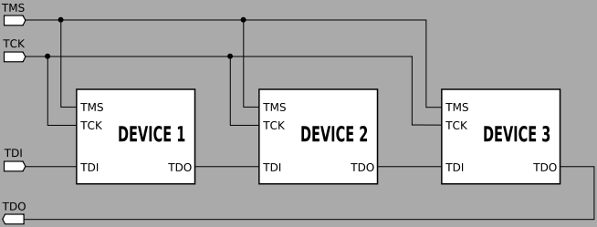
- Test Data In (TDI) is the input from the debugger
- Test Data Out (TDO) is the return end of the chain
- Test Clock (TCK) clocks this data along synchronously, similarly to SPI
- Test Mode Select (TMS) lets the devices know that they’re being debugged — it’s a global chip select
- Test Reset (TRST) is an optional signal that resets all devices in the chain
There are other signals as well, but they’re not standard and are mostly individual device resets. If you’re programming ARM chips, you’ll probably also encounter Serial Wire Debug (SWD) which is a two-wire simplification of JTAG where the TMS line is used for bidirectional data transfer (SWDIO) and the clock clocks (SWDCLK).
One Thousand Configurations
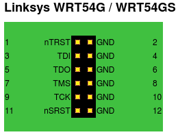
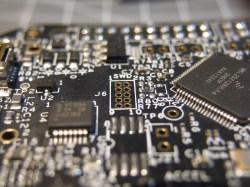
With only five signals, or a two-signal subset of these, you’d think that there were a limited number of possible pinouts. That would be naïve. You will commonly be presented with twenty-pin, fourteen-pin, and ten-pin versions of JTAG ports. Naturally, there are sub-varieties within each pin-count. Here’s a taxonomy of the ones that I’ve encountered. There must be others.
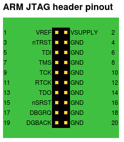
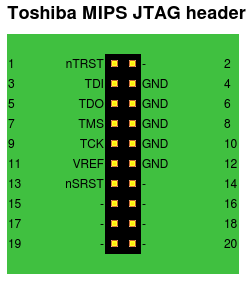
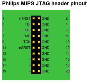
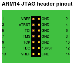
The madness started with ARM, when they decided to carry five signals on a twenty-pin connector. (To be fair, they added a few extra signal lines, and many redundant grounds.) This is also the only twenty-pin connector that I’ve seen, and it’s a good bet to start out with this pinout if you see two rows of ten pins. The two MIPS JTAG versions can also come in twenty-pin housings, but since they only use fourteen of them, they also appear in fourteen-pin versions.
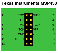
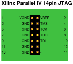
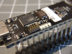
Which brings us to the first level of JTAG hell: fourteen pins. In addition to the ARM-14 pinout and the aforementioned MIPS variants, there’s also Xilinx and TI’s MSP430 JTAG layout in fourteen pins. Boo! There’s going to be some trial and error here. If there’s an MSP430 chip (or you’re using [Travis Goodspeed]’s GoodFET, then the TI version is most likely. If you see a Xilinx FPGA, that’s a solid bet. If it’s a router, bet on the MIPS layout first, but if there’s an ARM chip prominently in play you might want to try ARM-14.
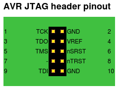
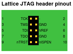
Which brings us into the pit of despair: the ten-pin headers. The good news here is the Alterra ByteBlaster and AVR pinouts match, and are maybe the most common layout of all. When I see a ten-pin header, I start here. Unfortunately, Freescale/Lattice semiconductor also has its own ten-pin JTAG, and it’s different, so that’s your next port of call.
Even that’s no guarantee though: my Lattice FRDM-KL25Z dev board has both ten-pin JTAG and SWD ports, where neither of the two correspond to any JTAG layout that I know, but at least they’re described in the datasheet. All of the other minor JTAG variants seem to be ten pins as well, so if you find a ten-pin header that’s not Alterra or Lattice, you’re in the deep end of the pool.
Which One Is It?
All of these connectors are, of course, symmetric. Once you’ve got a pin count and some good guesses, test them out. You should be able to figure out the grounded pins very easily with a continuity tester. Does it match any of the standards? If yes, you can figure out the orientation, and you’re on your way. If you know the chip manufacturer, start off with their JTAG version first, naturally. If you can trace known JTAG lines out from the IC, do so.
But then there are times when the connector is entirely non-standard, either because they designers don’t want you using it or they use a custom testing jig and don’t care. In these cases, it’s time to start playing the brute-force lottery. Take a wild guess at which pins are which, and see if you get a response. Repeat. And repeat. And repeat.
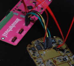 But if you’re a hacker, the words “brute force” make you instantly think “automation”, right? Among other devices, [Joe Grand]’s JTAGulator might be able to work out the pins for you.
It works by testing the JTAG chain, and when the pins are set up right, it’ll get a response. From this, it can figure out how many chips are in the chain, because each chip is essentially a one-bit shift register. Next it will ask for each chip’s ID code. When it starts getting sensible answers, you’ve won. Read [Joe]’s slides from his DEFCON talk (PDF) on the matter if you want to learn more.
Get Physical
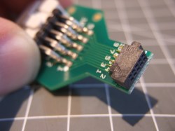
So far, we’ve only concerned ourselves with the signals that the JTAG pins carry. Without trying to obfuscate things, there are two choices of pin-pitch that are commonly used: the wide 0.1″ pitch and a smaller 0.05″ spacing. I’ve only ever seen ten-pin JTAG headers in the thin version, and they’re more common than the 0.1″ version. Before you even get to worry about programming the board, you’re going to need an adapter. And besides the pin-spacing issue, there’s also gender. You’re going to need more adapters.
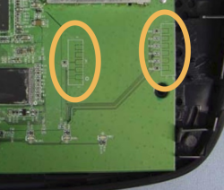
And then there’s obfuscation. Vendors who don’t want you using their JTAG interfaces once the hardware is in the wild will disguise them in every way possible. Even getting a probe on the right copper pads can be hard work.
Building Your Own
But what about designing JTAG into your own work? Which pinout should you choose? I default to the AVR/Alterra pinout in 0.1″ spacing whenever possible. One reason is that it leaves plenty of room for routing on home-etched boards, and the other is that it’s easy to drill for headers or leave bare copper pads for pogo pins.
For a pin jig on 0.1″ spacings, I’ll just jam the pogo pins into the end of a cable connector and try to steady my hands on the table while pressing enter on my laptop with the other, all the while playing the tuba with my toes. The pins will wiggle in the slots and I’ll curse. Reasonable people will resort to programming jigs, and there’s an app for that.
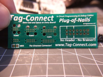
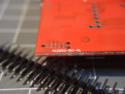
If you don’t have steady hands, and can’t be bothered with a test fixture, look into Tag-Connect. Tag-Connect is a simple idea: adding registration pins (and optionally locking tabs) in a non-symmetric configuration around a 0.05″ JTAG pattern. The registration pins make it easy to hold the pogo pins in place, and the locking clips give you your hands back. Instead of populating a header on every board you produce, you just need to expose copper pads and drill a few holes. It’s a brilliant system, and it’s been picked up by TI, Microchip, and others. A DIY version of Tag-Connect in 0.1″ pitch is on my short list of programmer connectors to standardize around.
JTAG: Love It or Loathe It
Love it or loathe it, you’re going to need to use JTAG some day, whether for your own designs and standardization purposes, for programming a dev board, or hacking into some appliance. It’s surprising that something so apparently simple as connecting up five signal lines can lead to such complication. The good news is that once you’re over this first hurdle, JTAG is actually reasonably well standardized at the protocol level. But that’s a topic for another time.






I’ve always wondered: if you used, say, IAR workbench, and had a FET programmer you would normally use for MSP430 processors, could you then also use that programmer to program for instance an ARM processor, for which there is also an IAR workbench version?
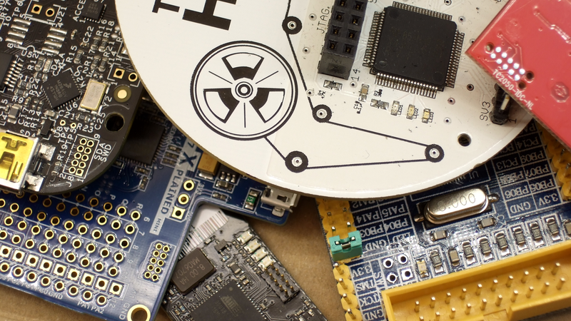
What does the reel pcb do? Can we get a closeup?
The Next HOPE badge. https://laughingsquid.com/photos-the-next-hope-hackers-on-planet-earth/
More details: http://travisgoodspeed.blogspot.com/2010/06/hacking-next-hope-badge.html
Thanks a million!
Good write up!
It would be nice to see the JTAGulator not only identify the correct pinout for a boundary scan header, but also implement a boundary scan chain controller (e.g. SVF player) with remapped pins.
On a more pedantic note (I know, I know):
“Test Mode Select (TMS) lets the devices know that they’re being debugged — it’s a global chip select”
The TMS signal controls the state transitions in the TAP controller – a little more involved than a chip select.
Came to comments to post about the TMS mistake. The article also fails to mention that the protocol was originally never intended for CPU debug, which is why every manufacturer does it differently. It was intended to do boundary scan – checking the board traces in an automatic way and making bed of nails obsolete.
Yeah, I wasn’t going to bring in the IEEE 1149.1 standard, which IEEE 1149.7 and IEEE 1532 used the same interface, as that would just muddy the already confusing world of JTAG (people’s use of the term), but that would be a more complete picture.
IEEE 1149.1 provides the ability for manufacturers to implement programmability, but no specification on how to do so.
Are there any worries about damage probing around?
Same question. But I don’t think so. The voltage is low and you don’t have power lines.
So at worst one may cause a system lock-up?
Mostly low risk, I’ve not used JTAGulator (when I was doing this I used my own programs, or had schematics) but TDO tolerates being grounded in my experience (might even be in the spec) and every port I’ve used has survived every abuse I’ve thrown at it. Most JTAG ports are 5v tolerent. TDO is usually easy to find because being an output it’s not pulled high or low and if you try pulling it with a high value resistor and watch on an oscilloscope, it doesn’t move. All the inputs move.
ARM chips are the exception. Usually 3v3 or lower and often not 5v tolerent. Some ARM JTAG debug connectors have such unbuffered lines and 12v input for enabling flash write (The Philips Shannon comes to mind which has/had a StrongARM), careless handling and putting 12v into the wrong line has fried many CPUs of people online.
Yes. You can trigger arbitrary commands in processors and anything else in the chain, so while you’ll probably just bork the running state (triggering a watchdog and resetting the processor, or setting the program counter to an arbitrary place), you could overwrite/wipe flash memory.
Iirc there are 1k series resistors in the JTAGulator. But this is of course not a guarantee that you won’t blow something up and as said you may lock the system or trigger commands.
“If you’re programming ARM chips”:
– If you’re using older (pre-Cortex) ARM chips then you’ll find RTCK which is needed because the TAP state-machine ran synchronously to an on-board clock so you needed to know when your TCK edge had actually been seen inside the chip
– nSRST is supposed to be “system” but few devices actually did the right thing with it if anything at all
– DBG* were a nice idea but even less well defined than nSRST so even less likely to do anything
– ARM have defined header pinouts at specific pin-pitches which is why you shouldn’t find, saw, the 10w header in anything other than 0.05″ pitch
I still wonder where the idea that SWD is a “two-wire simplification of JTAG” when the only relationship is that it re-uses the TMS and TCK pins.
Also I recall that I’ve used at least one ARM9 that had two scan chain select pins. One state of the chains was for on chip debug, the other was for boundary scan. I recall scanning through the register space and finding only BYPASS on the other two states. Only one of the chains had an IDCODE, which made things confusing. I’ve also used MIPS chips where the scan chain had two states, again debug and boundary scan, but that was set according to A9 (memory hazy – but literally one of the address lines) being tied with a high value resistor high or low on power up.
We also need standardized JTAG USB devices. Maybe there needs to be a new USB standard driver for JTAG devices.
If you get a Xilinx USB-JTAG interface, it will recognize non-Xilinx devices, but cannot actually program them or do anything useful with them except for get the vendor/device ID. If you want to program an Altera device, you need an Altera programmer, even though it speaks the same JTAG. This is STUPID! Why can’t you just have ONE USB-JTAG interface that can be recognized and used by any programming software that you care to use?
Just my quick little rant.
Most of the manufacturer specific JTAG adapters implement part of the programming protocol inside them for increased speed. As the programming protocols aren’t standardised, what works for one manufacturer won’t work for another. It should be possible to tell the adapter to go into basically passthrough mode but that again is specific to the adapter.
@GotNoTime: Whether “for increased speed” or “for vendor lock-in”, I’m not sure. What does Altera get out selling you their branded devices, using their software platform, etc? An engineer who only knows how to use one toolchain, and is reluctant to retrain on another for a day or two.
A setup like OpenOCD + a FT2232H breakout board with some EEPROM on it (which circuit in the FT2232H datasheet) is as capable as the software is, which is pretty good.
But yeah, chipmakers have different programming protocols.
I’ve seen 3 in 1 programmers on Ebay for $60 US that do Xilinx, Altera, and Lattice. The Xilinx platform cable knock off I use contains Cypress FX2 and a Xilinx XC2C256 so in theory it could be made into a universal JTAG.
There sort-of is, or at least could be – FTDI have a JTAG library for their FT2232H chip – I think Lattice and Xilinx programmers can use a 2232H for JTAG, though not sure if they use the FTDI library
Obligatory xkcd reference on standards:
https://xkcd.com/927/
Thank you for this article. You’ve saved me a lot of time. I haven’t implemented JTAG in my designs yet I’m sorry to say. Any references that you recommend? An edge connector has always seemed a reasonable place for a testing point.
I hope you are going to have follow up articles on this subject.
Does anyone have a JTAGulator equivalent that they use?
Better late than never/to others reading:
https://github.com/cyphunk/JTAGenum/wiki/Embedded-Analysis
JTAGenum is available as an .ino arduino sketch or Rπ bash script. If one takes a deeper dive into the reference materials at the above link, several other projects are referenced. Mr. Grand (JTAGulator’s designer) seems like a really nice guy. His site details the hardware all the way down to showing the BOM is around $50 to DIY. The only reason I haven’t considered building one (before finding JTAGenum) is because I have never played with Parallax. The .snap source I’ve seen looks very esoteric.
I’ve been doing this for 30 years now and never touched JTAG. I feel small, and a bit inadequate :(
But there are a lot of things I’ve never done or bothered to learn. Damn, what have I done with my life?
I really like the tag connect. We used it in a product about 10 years ago and it made updating firmware and debugging really easy. Saved our bacon when a firmware error cropped up.
The horror doesn’t stop there, unfortunately. In addition to the 0.1″ (2.54mm) and 0.05″ (1.27mm) spacings, you also got connectors with 2.00mm pitch. That’s when you start pulling your hair out and/or throw the board against the wall.
I’ve made a few devices with Freescale ARM micros lately…
I’ve been putting a 1.27mm header on with the same SWD layout as found on the freedom boards.
This allows me to use the frdm boards as programmers… see http://usbdm.sourceforge.net/USBDM_V4.10/Freedom/html/index.html
Maybe I shouldn’t be doing this but meh. Works for me. If volumes go up I’ll probably use a test/program bed of nails fixture and break it out to something a P&E cyclone or something similar can handle.
IEEE 1687 makes JTAG even more powerful for the system designer.
Speaking about JTAG, has anybody experience using the Bus Pirate 3.6 as a JTAG-Adapter? I am considering to buy one to mess with some old router and phones (and because it also looks like a nice universal interface). Does anybody know the shipping costs for Europe at seeedstudio?
The Bus Pirate works but is very slow. If you need to use it often then it will be frustrating. Get a Bus Blaster or similar FTDI based JTAG adapter if you need to use JTAG often.
Thank you! I never used JTAG, i just want to try it and tinker a bit with it, no need to be fast. I saw the Bus Blaster but it’s yet another thing to buy, while the Bus Pirate could be handy for other things too.
also the Bus Blaster doesn’t seem to be 5V tolerant.
Where are you going to run into 5V JTAG these days?
@asdf
Don’t know, but when messing around with undocumented devices you might find 5V, on a JTAG pin or even elsewhere (as i said, undocumented devices). Murphy is always looking for a good possibility to ruin your day…
Of course adding a “5V protector thingie” (just series resistors??) in front of the Bus Blaster shouldn’t be too difficult but it must be done…
@[asdf]
My Xilinx programmer is JTAG and it programs old 5V devices like CPLDs.
@RÖB:
Sure, if you have a supply of really old devices, but not for anything from the last 10-15 years. The XC9500XL is a 5V tolerant 3.3V device, and the Coolrunner-II uses 1.8V.
One of the above pictures shows the pinout for a Xilinx parallel cable. That’s a bit old now and isn’t supported by the current Xilinx software (even if you could find a computer with a parallel port).
The current Xilinx USB cables use a modified pinout. It’s mostly the same as the old pinout, with the following exceptions:
Pin 13 – Was GND, now PGND – signal from probe to board that lets the target board know that the probe is plugged in. The probe has an open drain driver on that pin. Typically it drives 0, but in theory you could set it high (open) to make the target board think the probe has been disconnected.
Pin 14 – Was open, now multifunction pin (refer to documentation). I’ve used this as an SRSTn from the probe to the target board.
Reference: https://www.xilinx.com/products/boards-and-kits/hw-usb-ii-g.html
You still can buy LPT peripheral PCI Express boards to put in any PC, and they will probably be with us, as an option, for quite some time.
I don’t get the point of this. I have heaps of JTAG interfaces like PIC, Atmel, ST, Xilinx, Altera etc and as far as I know they only work with the intended software that is aware of the driver for the JTAG box.
14 Pin JTAG headers with 0.05″ are uncommon? We must be the exception then, because we simply do not use any 0.1″ pitch connectors for any of our JTAG interfaces, be it 10-, 14, or 20 pins. And as for the pinout, we usually keep the layout the chip manufacturers have on theyr reference platform. Luckily we do not make massive JTAG-chains with chips from different manufacturers, or we could have a problem deciding what pinout to use for the chain…
JTAG is not debug, JTAG is not programming, at most JTAG is test, i.e. board components connectivity test also called “boundary scan”. JTAG is only communication layer to debug and programming as TCP/IP is to HTTP.
Saying “I can’t debug a device in my IDE over FTDI JTAG bridge” is like saying you can’t connect to FTP server with web browser.
Weird, since every microprocessor I’ve worked with since PIC16 has been debugged and programmed exclusively over JTAG.
Also, most web browsers can connect to FTP servers just fine.
Three from the top of my head that use different physical layer for transmitting debug messages: Cortex SWD, Tricore SPD, RH850 LPD, AVR debugWire.
Get this, there are DDRs with JTAG – what do you debug there?
I’m trying to point out that JTAG doesn’t specify debug operations. There is no JTAG defined register or operation that would stop the core, set breakpoint, read core register etc. JTAG is only one of mechanisms to transfer debug messages from debugger to device. How these messages look like and how many are needed for certain debug operation is up to silicon vendor.
Nowadays silicon vendors provide more than one physical way of sending same debug messages. E.g. Cortex-Ms have JTAG and SWD protocols on overlaying pins. This is to optimize the number of used pins for debug purposes.
Another analogy maybe, since you have web browser with FTP extension: SWD is like a motorcycle and JTAG is like a bus. They both get you from A to B just the ride is little different.
Unrelated fun fact: chips can (and do) have more than one JTAG device behind same JTAG pins. One is usually used for boundary scan and other is for debug.
Um SWD is just serialized JTAG.
It’s not. You can’t chain multiple SWD devices like you can multiple JTAG devices.
SWD is just another way of getting same debug (but not JTAG) messages across wires.
Like you can access same temperature, humidity and pressure registers on BME280 over SPI or I2C. Is I2C serialized SPI? Also neither defines temperature registers – because you can also use SPI or I2C to access EEPROM memory or sound codec.
And I imagine there are quite a few things you can debut on DDR memory chips, like reading out status registers or writing to command registers.
I also imagine that. But JTAG doesn’t define status or command registers. Just a way how they can be accessed.
Having seen ‘JTAG’ mentioned frequently, I was looking forward to enlightenment when I found this article.
Now that I’ve read it… my takeaway is that a person (like me) who mainly plays with a drawerful of PICs, ESP8266s and a few Arduino boards, and is only occasionally doing so for commercial gain or employment… will probably remain happier by ignoring JTAG.