Modified Yost Tames Pinout Plethora

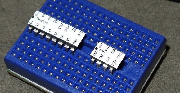
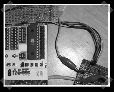
Every hacker has an assortment of USB to TTL-serial adapters kicking around in their lab, and we have all been annoyed that each one has a different pinout. You layout a PCB or breadboard for the Sparkfun flavor (GND, CTS, VCC, TXD, RXD, DTR), but when you begin troubleshooting all you can find is a CH340 board (GND, +5V, TXD, RXD, DTR, +3.3V). You have to jumper everything, and it becomes a mess. It wasn’t much better back in the days of RS-232 level signaling, either. While the pinouts were consistent, there were other headaches. Did the connection need a NULL modem adaptor? And if you were unlucky, you might need a DB-25 to DE-9 adaptor, and the really unlucky might need one or more gender changers. Surely there’s a better way.

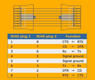
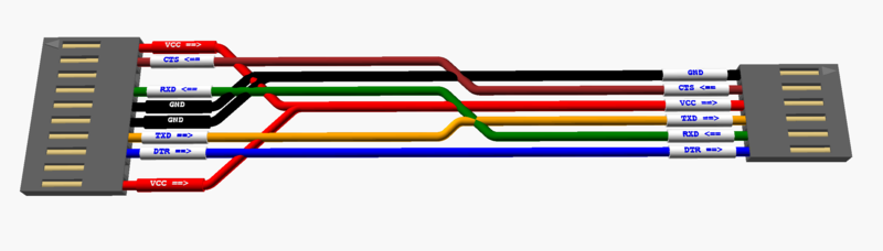
It turns out there was a better way, although it didn’t seem to have become as popular as one might expect. Back in 1987 [Dave Yost] formalized an interconnection scheme using RJ45 plugs and jacks while at Berkeley.  The signals were arranged in a mirrored fashion so that each cable is always a crossover — just plug two cables back-to-back if you really need a straight thru connection.

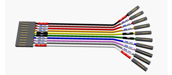
Even though he was dealing with RS-232 serial, nothing prevents us from using this scheme for logic level signaling. For example, consider the following 1×10 header pinout, where the original 8-pins are expanded to 10 to allow for power:

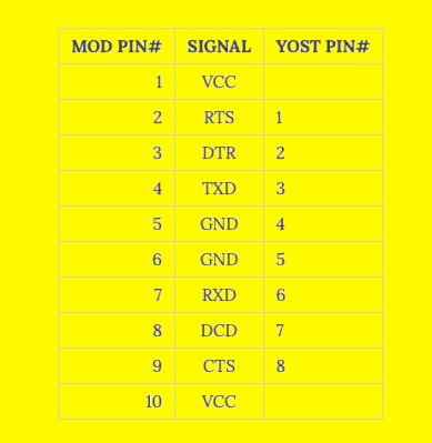
This is an extreme example, and can obviously be shrunk depending on how much handshaking, if any, or power is desired. Such a pinout lets you switch between DCE and DTE by simply flipping the connector around. And if a Dupont-style header slips off too easily in your applications, you could always use an RJ connector. This still doesn’t solve the Tower of Babel pinout problem with the USB-TTL adaptors. But standardizing on a serial pinout such as this for your projects and making cables or kludging your TTL adaptors will make serial debugging less painful.

Yost to Sparkfun Adaptor Cable

Back when he released this scheme in 1987, [Dave] pontificated:

“Maybe one day before the year 2,000, the world will have a new, simple, high-speed, flow-controlled, standard type of connection for point-to-point applications currently using RS-232, with an adaptor available to talk to old, RS-232 equipment.”

Let us know your thoughts in the comments below.

Why Some Chips Have Inconvenient Pinouts

If you’ve ever handled a chip with a really strange or highly inconvenient pinout and suspected that the reason had something to do with the inner workings, you may be interested to see [electronupdate]’s analysis of why the 4017 Decade Counter IC has such a weirdly nonintuitive pinout. It peeks into an IC design dating from the 1970s to see an example of the kind of design issues that can affect physical layout.

Inside the 4017. Want to make sense of how lines and shapes on a silicon wafer make an IC work? With the right teachers, it’s simple.

In the case of the 4017, once decapped and the inner workings exposed, things became more clear. Inside the chip are a bunch of flip-flops and NAND gates, laid out in a single layer. Some of the outputs (outputs 5 and 1 for example, physically on pins 1 and 2 respectively) share the same flip-flop.

The original design placed the elements in a way that made the most logical sense for routing and layout, which resulted in nice and tidy inner workings but an apparently illogical pinout. A lot of this is probably feeling familiar to anyone who has designed and routed a single-layer PCB, where being limited to one layer makes it important to get the most connections as directly near one another as possible.

Chip design has of course come a long way since the 70s, but there is forever some level of trade-off to be made between outward tidiness and inner design harmony. The next time you’re looking at a part with an apparently illogical pinout, there’s a fair chance it makes far more sense on the inside.

If any of you are interested in decapping ICs yourselves to see what’s inside, we saw that it’s possible with commonly available chemicals, not just nasty ones.

Continue reading “Why Some Chips Have Inconvenient Pinouts”

The Many Faces Of JTAG

Wouldn’t it be great if there were just one standard for attaching to, programming, and debugging hardware?  If you could just plug in and everything would just work? Dream on, dreamer! But of course we hobbyists aren’t the only people to suffer from multiple standards. Industry has the same problems, writ large. In response to the proliferation of smart devices — microcontrollers, sensors, and their friends — on any given PCB makes it difficult to test them all, much less their function as a system.

The Joint Test Action Group (JTAG) got together in the mid-80s to make automated testing of circuit boards a standardized process. A JTAG port can be found on almost any piece of consumer electronics with enough brains to warrant it, and it’s also a tremendously useful entry point for debugging your own work and hacking into other’s. You’re going to need to use JTAG someday.

Implemented right, it’s a very cool system that lets you test any compliant IC on the board all from a single connector. It’s mostly used by hackers for its ability to run and halt individual processors, and put them in debugging modes, inspecting their memory states, etc. Essentially every microcontroller responds to JTAG commands, and it’s an incredibly widespread and powerful standard. A victory for rationality and standardization!

The connector pinout was, of course, left up to the manufacturer. The horror!

Five Signals

In principle, JTAG uses five signal lines. They form a chain starting at the debugger, where one device’s output is the next device’s input, until the result is returned back to the debugger.

654px-jtag_chain
JTAG, as imagined by Vindicator CC BY 2.5
  • Test Data In (TDI) is the input from the debugger
  • Test Data Out (TDO) is the return end of the chain
  • Test Clock (TCK) clocks this data along synchronously, similarly to SPI
  • Test Mode Select (TMS) lets the devices know that they’re being debugged — it’s a global chip select
  • Test Reset (TRST) is an optional signal that resets all devices in the chain

Continue reading “The Many Faces Of JTAG”

Script Makes Custom Pinout Labels For Your Chips

cusom-pinout-labels

After years of prototyping hobby electronics we’ve learned (several times actually) that when something’s not working it’s a problem with the hardware. Usually the jumper wires aren’t hooked up correctly, or we needed to throw a pull-up resistor in and forgot to. One thing that can really help sort these problems out quickly is a pinout label for each chip like the ones seen above. This is a project which [John Meacham] came up with. It uses a script to generate chip pinouts on a label maker.

The label maker he started with is a Brother PT-1230PC. It connects to a computer via USB and can use a few different widths of self adhesive label tape. [John] found that the 1/4″ wide tape is nearly a perfect fit for PDIP components.

His script takes a YAML file as the input. This formatting standard makes is quick an easy to whip up a label for a new chip using just your text editor. From there his Pearl script turns the data into a Portable Network Graphics (.png) file with the labels spaced for the 0.1″ pitch of the chip. Send this graphic to your label maker and you’ve got an adhesive reminder that will help reduce the time you spend pawing through datasheets just for the pinouts.

Automatic JTAG Pinout Detection

Figuring out the JTAG pinout on a device turns out to be the most time consuming hardware portion of many hacks. [hunz] started a project called JTAG Finder to automatically detect the JTAG pinouts on arbitrary devices using an 8bit AVR ATmega16/32L microcontroller. Check out the slides (PDF) from the talk as they break down how one finds JTAG ports on an arbitrary device, with or without a pinout detection tool. [hunz] is looking for people to pick up the project where he left off.

Once you determine the correct pinout, you will need a JTAG cable: there are two main types, buffered and unbuffered, both of which I have soldered up and tested from these circuit diagrams (image of completed buffered cable here). The software most hardware people use today are the openwince JTAG Tools. To get the JTAG Tools to compile, grab the latest source directly from their CVS repository.

The last time we featured JTAG was with regards to Linksys devices, but the tools listed above can be applied to any device with JTAG.