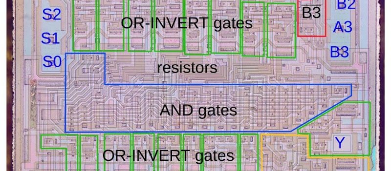
[Ken Shirriff] is the gift that keeps on giving this new year. His latest is a reverse engineering of the 74181 Arithmetic Logic Unit (ALU). The great news is that the die image and complexity are both optimized for you to succeed at doing your own reverse engineering.
 We have most recently seen [Ken] at work explaining his decapping and reverse engineering process at the Hackaday SuperCon followed soon after by his work on the 8008. That chip is crazy with complexity and a die-ogling noob (like several of us on the Hackaday crew) stands no chance of doing more than simply following along with what he explains. This time around, the 74181 is just right for the curious but not obsessed. Don’t believe me? The 8008 had around 3,500 transistors while the friendly 74181 hosts just 170. We like those odds!
A quick crash course in visually recognizing transistors will have you off to the races. [Ken] also provides reference for more complex devices. But where he really saves the day is in his schematic analysis. See, the traditional ‘textbook’ logic designs have been made faster in this chip and going through his explanation will get you back on track to follow the method behind the die’s madness.
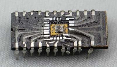
[Ken] took his own photograph of the die. You can see the donor chip above which had its ceramic enclosure shattered with a brisk tap from a sharp chisel.


I’m a noob to electronics. I literally didn’t know there was a dedicated ALU TTL chip out there. Fascinating. I wonder what I could do with that.
Arithmetic.
And logic
In a single Unit.
It’s the central part of a computer, so you could build a computer out of it. I’m not sure what else you could do with it, it has to be the most specialized member of the 7400 family.
The November 1972 issue of “73” magazine, available at archive.org, has an article about making a computer. It’s not a construction article, but sort of a map on how to do it, almost right before it all changed by the arrival of the microprocessor. The rare few did make them back then or scrounged up surplus, though most of the scratch built were fairly primitive. But this article gave an idea of what was involved, right down to explaining the ALU, though I can’t remember if it mentioned the 74181.
Michael
MIke ‘ALU’ is the acronym for Arithmetic Logic Unit.
Yep, looks like that error was introduced during editing. Fixed!
Any chance we (I) could get an explanation of exactly how multi-emitter transistors work? I’ve never quite understood how (if) they isolate the multiple emitters from each other.
Multiple-emitter transistors aren’t as tricky as you might expect. If you look at the NPN picture in my article, just stretch out the transistor and drop more emitters onto the base. The emitters are isolated from each other by the base’s P-doped silicon. It’s kind of like taking a bunch of transistors and connecting their bases and collectors together, but more efficient on the die to have one transistor with multiple emitters. The other way of thinking about the TTL multiple-emitter transistors is they are a lot like back-to-back diodes, and each emitter adds another diode.
Sometimes it is hard to grasp IC internal circuitry, since there are limits to what they can put in (no large value resistors, with some exceptions no capacitors), so the circuitry cm be roundabout, lots of transistors, which are cheap, to compensate. What works in ICs aren’t necessarily the best choice if building with discrete components, so things like those multiple emitters appear. If a use could be found for them, I’m sure there would be discrete transistors with multiple emitters available. Actually, I remember there were RF power transistors with multiple resisters, I think those were multiple transistors inside the can, the multiple emitters for balancing purposes.
Michael
awesome. Cool BJT “tricks” in there, too.
The walkaway as someone mentioned previously is that going from photo to schematic is a lot of manual work. Surprised none of the big names with their machine vision work hasn’t come up with something to make things easier.
What was that chip opened with? A nuke?
From the article, it was a ceramic package, so he used a chisel.
“scuze me? REVERSE ENGINEERING of the ‘181?
Data sheets from RCA, Harris (4-bit CMOS), TI (4-bit TTL), IDT (16-bit CMOS), and many others are freely available. Simply grab yourself some simple gates and plagiarize away.
What’s the big deal? TI’s data sheet gives you THE EXACT SCHEMATIC of the 75-gate ALU.
I have a feeling you’re missing the big picture. It isn’t THIS particular example, but of gaining the knowledge and experience that can allow one to apply to OTHER chips out there. The datasheet is like the answer key to a test. It tells you after going through the process that you got it right.
These ICs have so little complexity. Even the most simple of ICs designed these days are much more complex and are most likely CMOS especially if digital.
If the goal is to know more about how chips are designed, I recommend reading a text on IC design and searching for academic papers on the subject.
I respectfully disagree. Taking the time to take apart a simple chip like this is better than any lab that I had in undergrad. And, as [jawnhenry] points out, you can use the datasheet when you get stuck.
I’m more pro-book-learning than many, but there’s a lot to be learned from working through a good simple example yourself. This is awesome, and I hope it inspires some folks to dive in. Thanks, Ken.
When you read the datasheet you see only what the manufacturer wants you to see: In this case a simplified gate-level diagram.
A detailed transistor level diagram often reveals implementation secrets not readily apparent such as test structures, undocumented features, hidden registeres, etc. That’s why manufacturers reverse engineer each other’s chips… And also to check on infringement and competators technology.
On the MC68000 there are sense amps for connecting buses, and undocumented conditions that allow the on chip microcode to be dumped for testing.
The uPD765 floppy controller has similar DMA-related conditions that dump it’s microcode.
Ken has documented the unanticipated 4-but ALU of the Z80 that is not documented along with additional instructions.
An SMC baud rate generator uses programmable dividers to select various baud rates. An examination of the die reveals these to be polynomial counters–fast and area efficient to implement.
All we can say on Ken’s work is BRAVO! …
I really enjoyed reading how Ken Shirriff was dissecting and explaining architecture and design of 74181 4-bit ALU, a marvelous work. No technical reference, datasheet, book or guide so far showed so detailed and clear technical insight in 74181’s design as his latest reverse engineering work does.
Although we all for years know well and use those IC’s , some inner working and architectural solutions was hidden in “black box”… until now :)
Ken Shirriff, thank you very much :)
Which came first, the FSC 9341 or the TI 74181?