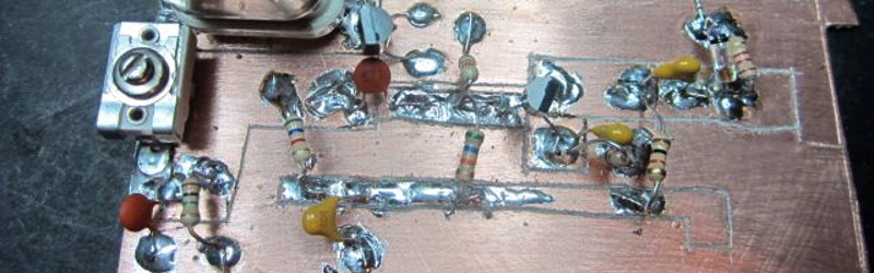
There are a variety of techniques employed by electronic constructors seeking the convenience of a printed circuit board without the inconvenience of making a printed circuit board. Dead bug style construction in which the components float on a spiders-web of soldered leads above a ground plane is one, Manhattan style construction in which pads made from small cut squares of bare copper-clad PCB are glued on top of a groundplane is another.
[Freestate QRP] has another take on this type of electronics, with what he calls “Scribble style” construction. He cuts away copper from bare board to create pads and rudimentary tracks, and for him the magic ingredient comes from his choice of an engineer’s scribe to do the job. This is where the “scribble” comes from, creating a pad is as simple as drawing it with the scribe.
Of course, this technique is not entirely new, constructors have been doing this type of work for years with Dremel tools, hand engraving tools, and similar. If you’ve ever tried to do it with a knife or scalpel you will know that it’s hardly an easy task with those hand tools so the prospect of another one doing a better job is rather interesting. He’s ready and able to demonstrate it in action, showing us a couple of RF circuits using the technique.
Have you tried this technique, or one like it? How did you get on, tell us in the comments. Meanwhile, you might like to read our own [Dan Maloney]’s look at dead bug and Manhattan construction.


I’ve done a few this way… sometimes with a hacksaw to score up the PCB into zones.
The downside with this approach is doing SMD with anything more advanced than discrete components is basically out.
How about you post and show us all how its really done instead of just being a douche with a worthless comment?
Good on ya FQRP, still learning Manhattan style here, so very interesting approach that I’ve not seen yet! I gotta admit that Redhatters comment about using a hacksaw seems like a much quicker and cleaner approach. Still great to see something new to me!
Prototyping as it was done decades ago! Blast from the past.
Sloppy some say? That’s only cause it was a quickie ckt slammed together FAST to test with and needs plenty of room and big blobs of solder to quick slop tack this or that test component onto AND remove easily… fudging till it works good. Later will make one that’s purty and has holes for the leads. Fully valid and often seen method for on-the-fly engineering in the day of slide-rules instead of calculators. Faster to know the formulae and ESTIMATE the component value needed and solder it in then test… than it was to sit down with the sliderule and manually do the calcs. Once you do get the prototype working fine you capture the schematic onto paper then one time go through all the calcs by hand and refine the component values further.
I guess we’ve lost something over the yrs.
Maybe that’s why there are so many old radios out there with known mods.. change the value of this or that resistor or capacitor and performance becomes much better!
As someone with a math degree and electrical engineering minor, I can confirm that what you describe is the technique favored by engineers.
It used to frustrate the crap out of me because it was slower and less accurate, make a ton on invalid assumptions that lead to poor engineering design, and is just a horrible clunky way to try and do something where in the end you get a half-assed design that semi-works on the bench and fails in the field. But it saves the engineer from having to actually understand the concepts involved or learn to do math.
I found it even more odd because these engineering profs love to talk about the slow iterative trial and error clumsiness of builders before true engineering came into its own in the 1700’s with iron structural elements, when they could for the first time use mathematical modelling to create a perfectly designed system. Then they just fall back on trial and error in the 21st century anyway when they have endless cheap computer power.
There’s a large distinction between structural designs and electronics designs: structural work is extremely expensive and fairly simple to calculate, electronics is pretty complex to calculate, but dirt cheap to build (or modify).
Rest assured, buildings and bridges still get calculated in every detail before one even thinks about ordering material. A $2million “prototype” can’t be simply thrown away.
When doing an entirely new electronics design I usually make prototyping PCBs. Not sure how big a capacitor should be? Well, add space for three of them in parallel or at least sufficient space for the largest one. Not sure which filter principle works best? Add both. Often even with jumpers to change the design without soldering.
Having reasonably quick prototyping equipment allows to do this. Once the best electrical design is found, all the then surplus stuff gets removed from the PCB layout and another board is made.
As I said, my degree is in electrical. The structural stuff was just the historical anecdotes of how wonderful engineering is. The only things I know about structural engineering is what I’ve learned watching the great courses series.
My point exactly is “not sure which capacitor works best” “well this one is working perfectly in my lab so lets go into production with it” Now we deploy 10,000 boards into the field at -20 or +140 degrees and we can’t figure out why the design doesn’t work. Now when the electrolyte has aged 15 years all the boards are failing…wonder why. You suggesting trial and error on filter principles is just making me cringe.
And I know full well in the “real” world a terrifyingly large amount of design is done exactly as you’re saying. And that’s why so much of the stuff out there is crap that never works properly. Back before designs were so integrated and specialized I used to get a lot of my parts by buying surplus electronic devicess that were brand new, and utterly flawed in design to dismantle. Some of them I even fixed the design flaws; I remember a pretty nice light display system I bought where the controller box got super hot and let out the magic smoke after about an hour of operation. Once I replaced the under-rated transistors everything was good. This was a manufactured product in high-end retail packaging, it must have been worth $200 and I paid $5 for it; somebody lost a fortune off that design.
The math is very well understood and very simple if you actually understand the concepts.
” Now when the electrolyte has aged 15 years all the boards are failing…wonder why.”
Yes, especially since it was supposed to fail after 2 or 3, whenever the warranty is out!
“Once I replaced the under-rated transistors everything was good.”
That’s no unique story. I used to work at a radio station. There were papers you could subscribe to that would tell you when things like this were discovered. The best way to get reliable equipment… it’s not to buy new. Instead dig some popular, well-known model device out of a garage sale or flea market. Look it up and see what part substitutions have been suggested over the years. Perform them.
Also, visually inspect the capacitors for bulges and the PCB for discoloration. Replace the bulged capacitors. Where the PCB is discolored there is probably a hot resistor that should be replaced with a higher wattage version and maybe with some long leads to help get it up and away from the PCB where it can air out.
Once you have done this you have a device you can rely on for a long time.
I wasn’t talking of the newbs back in the day, was referring to the established amatuers that actually understood the electronics and breathed the formulae. MARS sat, EME, talking skip, 300 ft antenna masts, etc… And it was the days of sliderules not calculators. Calculators were years in the future. Digital electronics didn’t exist unless you counted relays and steppers. Days where copper clad board folks were just figuring out how to use and chassis were point to point assembly, resistors and L/C components hung in air bridging the gap from one tube output to the next tube input. 5 yrs old an dad dragging me from one ham meeting to another, getting me outta way by letting me play with scope showing lissajou.
You guys missed the good days! You can do a lot more now… but there ARE NO MORE COWBOYS.
It’s still trial and error even if you move the trial and error into a computer instead of on the board.
It’ll get worse though…
Siri! Design me a boost buck regulator for 1.5 volt to … … … in 5 components or less and .5 cubic inches or smaller … and have XYZ assembly house make 7 and ship overnight.
Those after us won’t need to understand… and won’t.
It’s TI webench you are referring to I assume?
A few more methods from W2AEW:
https://www.youtube.com/watch?v=kH110yjYZ2g
I do this all the time too, but with a ruler and an acrylic-scoring blade in a matte knife. Takes 4-5 passes to get a line clean, but it also doubles as a PCB cutter — score on both sides and snap. (Which I guess is what it’s intended for…)
With a ruler and a pen for layout, you can “easily” Manhattan up SOIC-8s this way.
I’m going to go check out engineer’s scribes. And maybe engraver (artist) copper scribes too, while I’m at it. Thanks for the inspiration.
Please. We’re in 2017, where a design is done in a PCB layout application anyways and exporting G-code from there to get the stuff milled on a $200 milling machine is a matter of a few minutes.
Not everyone has access to those tools, can afford them, or even wants them. I have created some of my own test equipment using similar methods to the one shown here, and the total cost was minuscule.
As far as the software tools, there’s an endless list that’s free or free for hobbyists. In 2017 it’s cheaper to have the board made on that $200 million milling machine than to buy the blank board. The software/commercial build is also much faster and easier to do, but there will always be people who think it’s easier to hack away and a problem by brute force than learn to use a tool.
All that said, while the technique is completely useless to assist with dev or design these day, this is hack-a-day, and encouraging people to play with it for its own sake isn’t such a bad thing.
Made? Sure. Shipped? It depends. Also, having your boards shipped to you for a couple of months minimum is not worth it, especially when all you wanted is a small batch of boards.
Yet, some people are just getting into this field. To expect someone to put down $200 on a milling machine for their first few PCBs is a little far fetched. I could see it going like this.
New Engineer – “Hey Honey, I’m going to buy a $200 PCB milling machine.”
Significant Other – “What are you going to make with it?”
New Engineer – “Remember I showed you that blinking LED? I want to make it a permanent circuit”
Significant Other – “Yes, I remember. Why don’t you spend that $200 on the family instead of a toy.”
Excellent story!
Good thing I can spend mine on whatever.
That sounds like more of a spouse problem than a technology problem.
Be real man. Almost every relationship is a constant struggle to maintain *some* of your freedom.
milling PCBs is a terrible solution, it’s far lower resolution than photoresist + etch
Can’t be more terrible than etchant. But can also do drills, cuts and 3D milling in general.
But… but… this guy still has $200, and got ‘er done! And all the milling machine does is “make it look purty!”. I don’t think there is a single electron in the whole universe that would notice the difference!
If I gotta pick one or the other that made a mistake here…
i just did another toner transfer board and it works. it was kind of a tie in for my pi tablet, to tie together a charger pcb, a battery (3 18650 cells in series), smps, and an audio amplifier. all standard chinese ebay fare. also a diode and pfet isolation circuit to keep the pi powered while its charging. also carries an attiny85 to monitor the battery voltages and communicate it to the pi over serial.
its not bad for a 2×2 board though i could have got it smaller if i had more surface mount parts (so far only the pfet and a 3.3v ldo for the 85, was going to use a spare tqfp 328p i had, but opted for the 85 dip instead as it had everything it needed).
i suppose if you want a board right now the cut n connect system might work, though i usually go for a proto board if im gonna go the lazy route.
> i just did another toner transfer board and it works.
Once you’ve gone photo-etch (or transparency-etch), you’ll never go back to toner transfer. One more “wet” step with NaOH to dissolve the exposed coating, rinse, and etch. I use a “screw” type blacklight CFL for 10 minutes at about 3-4″, works perfectly every time.
Any link to ebay or so?
I’m a big fan of this method. I use an OLFA box cutter with an angle attachment and it goes quite fast. Good down to ~0.8mm pitch, which covers larger SMT parts.
https://cdn.hackaday.io/images/2497651482345483168.JPG
Uh, one more:
https://cdn.hackaday.io/images/6095341469915470257.JPG
Rear view showing the box cutter pulling up a satisfying curl of conductive debris:
http://i.imgur.com/2uShrZi.jpg
this are beautiful!
That is indeed nice work!
Simon? Classy! Beautiful work.
Very impressive. Great job!
I’ve done it with a “Dremel tool”, using one of the cutting bits. Worked fine, no worry about having press too hard and ending up cutting yourself. It’s probably easier to add things once some circuit is in place, it’s easier manipulating the cutting bit than a utility knife.
Remember, this gives you a good ground surface. For lots of reasons, including etching time, an etched circuit board may have little etched space, and this becomes the equivalent.
Michael
I have made my fair share of LNAs, Mixers, LOs, filters, exc using this method
Using a scribe was taught to me in 2004 as a kid
Actually, I have done this few times and I have found it to be quite neat, robust and pleasant :)
The key ingredient is PCB substrate/producer. For microwave circuits I was using Rogers 4003 and it was very easy to remove copper just with a tape knife, using metal ruler along gave really neat results.
Life simply doesn’t always give you PCB shop or milling machine.
Lots faster too!
Don’t get me wrong. I definitely think it is good to have the skills to do something like this yourself. Also, with a simple design it might be far more time efficient to just do this with a scribe, dremel or whatever one’s favorite tool is than to draw it up in a CAD program and etch it on a mill. I have lots of blank, non-UV activated copper PCB and intend to use much of it in this way.
But.. there are always people who get on here and wine about not having access to a mill, a laser cutter, a 3d printer, etc… I wonder how many of those complaints are really legit. I consider the area I live in to be pretty much a thechno geek black hole. It’s far from Silicon Valley and offers little to one with such interests. And yet… I know of 3 hackerspaces, 2 of which have public hours for non-members and at least 2 maker tools-equipped library systems within a 35 minute drive of my house. Bump that up to 1 hour and I can include 2 more hackerspaces and a Micro Center store.
Are people really unable to get access to equipment? Or just too lazy to travel a little?
Not everyone lives in America, you know. Despite this song :
https://www.youtube.com/watch?v=Rr8ljRgcJNM
With 45 years of circuit design for production, I don’t understand basing production on nominal value calculations. I have always made worst case calculations using maximum, minimum and nominal values including an estimate of drift at maximum, minimum and room ambient temperatures. I would also calculate the maximum voltage, current and power dissipation and/or temperature of each component. This is time-consuming, but my circuits rarely failed. After doing this I felt like I really understood the circuit. I did usually make a breadboard based on nominal calculations and make the worst case calculations after I saw it work. I also do a spice simulation before the breadboard if it doesn’t require too much tweaking of the simulator. For a one-off, I usually don’t do all of this. Making all of these calculations is much easier with MathCAD or Smath Studio, and these documents would go to the client so that, if there was a problem, anyone could go in and see the effects of a change.
Maybe as a way to produce cheaper?
Or.. maybe it IS supposed to fail. They want the customer to keep coming back to buy replacements don’t they?!?
forcefully deleted
*Jenny List style