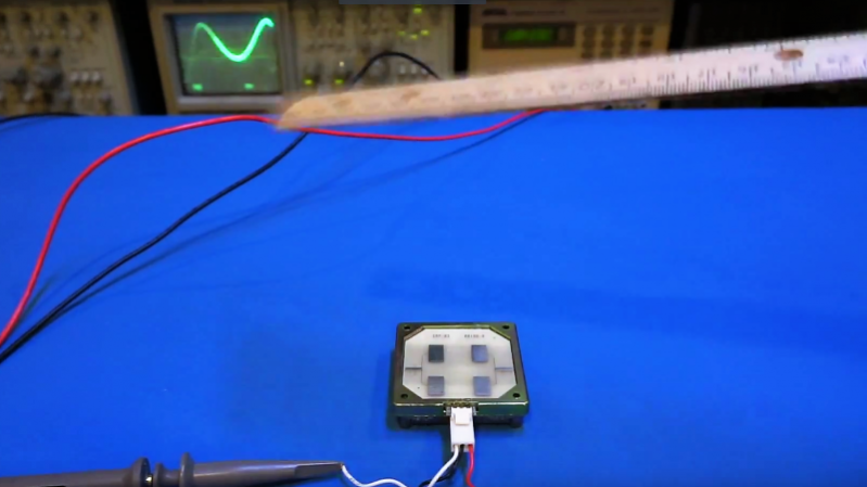
Oscillators with components that aren’t electrically connected to anything? PCB traces that function as passive components based solely on their shape? Slots and holes in the board with specific functions? Welcome to the weird and wonderful world of microwave electronics, brought to you through this teardown and analysis of a Doppler microwave transceiver module.
We’ve always been fascinated by the way conventional electronic rules break down as frequency increases. The Doppler module that [Kerry Wong] chose to pop open, a Microsemi X-band transceiver that goes for about $10 on eBay right now, has vanishingly few components inside. One transistor for the local oscillator, one for the mixer, and about three other passives are the whole BOM. That the LO is tuned by a barium titanate slug that acts as a dielectric resonator is just fascinating, as is the fact that PB traces can form a complete filter network just by virtue of their size and shape. Antennas that are coupled to the transceiver through an air gap via slots in the board are a neat trick too.
[Kerry] analyzes all this in the video below and shows how the module can be used as a sensor. If you need a little more detail on putting these modules to work, we’ve got some basic circuits you can check out.


Writing a bit too fast again? The sentence “That the LO is tuned” is weird, and what’s “PB traces”?
LO == Local Oscillator
PB possibly for the poisonous lead material… or ParaBolic traces (Reflective tracks/traces?
That’s what I’d guess…
Good article, I’ve nothing to complain about.
Yet to watch the video properly
I was thinking they might have meant PCB
Relax.
The first one is just an instance of inversion, for emphasis. To me (disclaimer: non-native speaker) it looks like perfectly correct English.
PB traces == printed board traces
You are correct, and the sentence in the article is also.
(native English speaker)
Just checking something….
LO == Local Oscillator
PB possibly for the poisonous lead material… or ParaBolic traces (Reflective tracks/traces?
That’s what I’d guess…
Good article, I’ve nothing to complain about.
Nicely put together video as well.
Sent via a h4x0r’d Veh Pei Ehn
Quote:
“Sent via a h4x0r’d Veh Pei Ehn”
Now… via Tor and a VPN.
As a test of the comments section…
Great tear down video. Rf terminology is also extremely weird and rather ad hoc . I am under the impression that 10 GHz would be called “millimetre wavelength” rather than microwave?
Both or either, depending on who you’re talking to.
Of the folks that I know and are doing millimeter wave stuff professionally most refer to stuff with wavelenghts below 1cm (10mm) to be millimeter waves as it’s single digit millimeters. So 10GHz at 3cm and 24GHz 1.2cm are not millimeter waves, but that’s just how things are.
Moment to remind me of where confusing physics and RF Engineering terminology starts taking over. Then things turn into Reciprocal Centimeters in the IR range for units versus Nanometers. You never really see Hertz used past the TeraHertz range and Microwaves are not referred to past 300Ghz in my experience. Then everyone seems to act like there is nothing higher than Cosmic Radiation and I’m not sure what the unit are. Maybe CERN has a scientist or two I’ve read before like once. The higher the frequency the more deniability of existence of systems and confusion starts kicking in along with disinformation tactics. The only exceptions are RF hearing in the sonic range. From RF to Microwave hearing seems to be acknowledged if you really read up… otherwise cochlear implant surgeons get angry I guess?
Another strange transition I find that is not clear is the particle transition to the forces; i.e. gravitational, electromagnetic, weak and strong forces. Is the muon and tau magnetic also?https://en.wikipedia.org/wiki/Muon_tomography
Part of my ambient conditions theory of using neutrinos to perform harassment or at least more than with the electron, the muon and tau may be able to be used in systems we don’t know about.
Null Post to access the other post for a copy+paste now an I–P Bhan is bypassed by a nice Veh Pei En change…. The haqed corp/LTD has changed ISPs and… It still called back home….
Nice video. HP8566B is an extremely nice SA. Hope I can keep mine running for a while longer. Just a couple of observations after watching the entire video. For anyone wondering about that really high epsilon-real (Er=30) for the DRO calculation, that isn’t because of the pcb material, but because of the ceramic substrate that the DRO is constructed on. That keeps the circuit compact since the the velocity of of EM propagation in vacuum ratio to velocity in the dielectric is slowed by a factor of the square root of Er. Also, I didn’t really understand why the claims about copying of design? Radial stubs and low-pass filters in distributed-component form are going to look very similar from design to design at that frequency. I didn’t really see why he claimed that. Also, very cool how the antenna structure was coupled through the pcb by slots / air-gap. I would think there was quite a bit of loss in that coupling. Would be fun to simulate that and see what the expected loss would be. Nice find.
Just mind your back and lift with your knees should you ever need to move that 8566B(east)!!!
I’m looking across my work area at a R&S 40 Ghz SA that still has a 3.5 floppy drive in it right now and can almost lift it with the Jedi mind trick as compared to that old HP beige monstrosity! But its still a good unit, just ancient and heavy as a boat anchor!
I cant watch the video, but transformers and chokes are some times air coupled, as are caps. also waveguide is a hollow tube and has lower loss than coaxial cable, but being down in X-band, I’m not so sure this would equate to wave guide as x-band waveguide would ideally be much larger. perhaps the sloting is doing some sort of circulator magic to keep tx / rx isolation since this is a CW unit? but you might expect they wouldn’t be looking to grab the carrier on return as much as the Doppler frequency itself. Microweird?
Mine stopped working with several problems a couple of years ago. The Video and switches were fine, just the intelligence went wacky. I had fun tearing it apart. I found the programmable attenuator switch to be very useful. Getting rid of the power supply reduced the weight by half.
Well, the barium titanate is like lithium titanate and used in super capacitors I know. The barium is the cheaper and not as effective material based on material mass and volume, i.e. particle size since you want the largest surface area from smallest size particle if I understand correctly to store the most electrons.
So does the barium titanate couple charge and de-couple discharge with the transistor to the breakdown of the transistor to create the oscillation (I might be explaining that wrong like the collector ground voltage is high enough once the capacitor is charged to make the transistor emit with a known frequency based on size of capacitor) or is it coupling to smooth out or stabilize another oscillator from the transistor breakdown or somehow I don’t understand enough?