The idea of making your own semiconductors from scratch would be more attractive if it weren’t for the expensive equipment and noxious chemicals required for silicon fabrication. But simple semiconductors can be cooked up at home without anything fancy, and they can actually yield pretty good results.
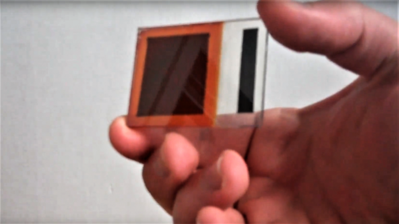
Granted, [Simplifier] has been working on the method detailed in the video below for about a year, and a look at his post on copper oxide thin-film solar cells reveals a meticulous approach to optimize everything. He started with regular window glass, heated over a propane burner and sprayed with a tin oxide solution to make it conductive while remaining transparent. The N-type layer was sprayed on next in the form of zinc oxide doped with magnesium. Copper oxide, the P-type layer, was electroplated on next, followed by a quick dip in copper sulfide to act as another transparent conductor. A conductive compound of sodium silicate and graphite was layered on the back to form the electrical contacts. The cell worked pretty well — 525 mV open circuit voltage and 6.5 mA short-circuit current. Not bad for home brewed.
If you want to replicate [Simplifier]’s methods, you’ll find his ample documentation of his site. Of course, if you yearn for DIY silicon semiconductors, there’s a fab for that, too.


Who else had the Lindsey Electronics book about this!? I miss those wonderful catalogues..
I’m impressed by how well that link looks on mobile.
Not to mention the nice native font.
Also nice project.
Have now watched production of a coin cell and a solar cell using a razor blade cutting lines – starting to think great invention has been by way of excessive drug abuse. [enters dark web to genius up]
What a beautiful job he did. Considering the very small size of the cell, that is a very decent output I believe. Would not be hard to make a bunch of them and wire some in series and some in parallel to make a very usable output. Excellent documentation too.
The same guy’s work on conductive glass (https://hackaday.com/2017/03/20/diy-conductive-glass-you-could-actually-make/) is also marvelous, and related. You should really check that out too.
Check out the entire site… I just spent hours reading page after page.
While I don’t see myself making my own triodes and pentodes, it was interesting to see the processes evolve.
Giving the output without the size is kind of useless. For the output and the amount of work involved I would look into making a thermopile out of common wire materials.
from the picture i estimate it is 1.5 in square, or 2.25in^2. from handling them, i estimate a commercial 300W panel is about 15ft^2. long story short, i think it is about 1% as efficient as the modern commercial panels.
not to disparage — it’s a fantastic accomplishment! it’s just that the back of my envelope doesn’t inspire me to use it.
of course, without watching the video, i can’t tell you what light source he used, so maybe in full sunlight his would be closer to the state of the art..
I did a rough calculation of output compared with industry standards, assuming the sample was tested at 1 sun output at standard conditions.
.525 volts per discrete cell is almost that of mainstream polycrystalline solar cells, and remains constant as cell size changes (all other things being equal; scale up of size can result in degradation of output due to other things than inherent efficiency).
a 1.5 inch square cell is .00137 Sq. M.
A standard silicon cell is 150mm square, or .0225 Sq. m.
There are 60 cells in a standard silicon solar module, or 1.4 Sq. M.
Therefore a solar module is (.0225/.00137) * 60 = 985 times larger in surface area than the sample.
If the sample were the same surface area as a standard solar module, the output would be 985 times larger as well.
985 * .0065 = 6.4 amps
A module of standard surface area, but with the copper chemistry would be 6.4 amps, and (.525*60)=31.5 volts
Overall power is roughly 6.4 * 31.5 = 202 watts
A typical polycrystalline module today is 34 volts * 8.4 amps = 286 watts or so
So, 202 watts compared to 286 isn’t bad!!
Of course scaleup is always difficult, no matter what the PV technology. However, I salute one with relatively low embodied energy compared to silicon, and created in a low tech environment!!
I think you’re being a bit generous here; an easier way would be to just compare the characteristics per square centimeter. IIRC silicon produces around 30mA/cm², at a slightly higher voltage with a far higher fill-factor (squareness of the I/V curve). I don’t have a way of accurately simulating “standard” sunlight so I can’t be 100% certain, but I’d guess my cells have an efficiency of around 0.1-0.3%, compared to 15-25% for commercial silicon cells. 1% of a modern panel sounds about right.
The size is specified in the article on my site. The solar cell is 3in² overall, and the active area is 7.5cm². A wire-based thermopile that produced the same amount of power from sunlight would be several orders of magnitude larger, heavier, and more expensive.
What would be really impressive is making multiple cells like this on a single, large sheet of glass. Make them in a series-parallel matrix to boost both volts and amps so it has an output that’s actually useful.
That’s what’s done with commercial thin-film cells. The lines you see on the front of them aren’t current collectors, they’re inter-cell connections. Each cell is a long strip for minimum resistive losses through the conductive glass; 10 ohms per square isn’t a big deal if you’re only using a thin slice of that square. I considered doing that, but the complexity of the masking/etching processes would have overshadowed the simplicity of the overall concept. I might come back to it later though.
Nice video, but I wish you had labels on the beakers of CuS. It looked at first like water.
The small beaker was labeled earlier in the video (Na2S, not CuS), and the larger beaker in the dipping shot actually was water. I considered labeling it, but I had already mentioned it in the article and figured that would be enough for anyone trying to replicate the procedure.
I hope we get to see more like this. Solar cells need to go through the same thing personal computers went through in garages all over the world. Very cool.
Looks like this guy is using something similar to spray pyrolysis, which is certainly accessible to hobbyists if they’re chemically oriented like this guy. Inkjet printing is also a pretty accessible method for making solution-processed devices, and far easier to make fully integrated circuits – not on the same nanoscopic scale as with photolithographic processes, but with the right hacks to a regular inkjet printer anyone could deposit electronic materials with enough accuracy to build circuits with a transistor density on the order of a few per mm^2 or so.
I was chemically curious in college.
Well done sir!!!
I discovered by accident that the commutator of small dc motors also seem to build up semiconducting copper oxide that works as a diode for a crystal set reasonably well.
Maybe something in this to easily make small amounts for experimentaiton without the need for any chemicals or flame etc.