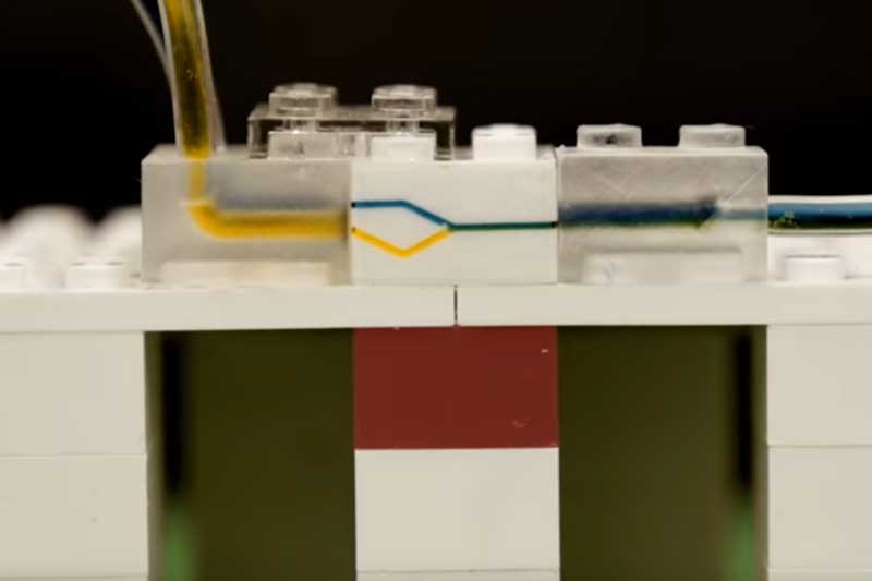
As any good hacker (or scientist) knows, sometimes you find the tools you need in unexpected places. For one group of MIT scientists, that place is a box of Lego. Graduate student [Crystal Owens] was looking for new ways to make a cheap, simple microfluidics kit. This technique uses the flow of small amounts of liquid to do things like sort cells, test the purity of liquids and much more. The existing lab tools aren’t cheap, but [Crystal] realized that Lego could do the same thing. By cutting channels into the flat surface of a Lego brick with a precise CNC machine and covering the side of the brick with glass, she was able to create microfluidic tools like mixers, drop makers and others. To create a fluid resistor, she made the channel smaller. To create a larger microfluidic system, she mounted the blocks next to each other so the channels connected. The tiny gap between blocks (about 100 to 500 microns) was dealt with by adding an O-ring to the end of each of channel. Line up several of these bricks, and you have a complete microfluidic system in a few blocks, and a lab that only costs a few dollars.
Of course, there are limitations. The ABS plastic Lego bricks are made from can’t handle chemicals like organic solvents, and the channels can’t be smaller than about 10 microns wide, which is too wide for some microfluidic techniques. These issues aside, it’s a great and inventive idea, and MIT is currently working on a web site that will show you how to make your own Lego microfluidics lab.


Laser engraving could achieve smaller channels
You dont want to laser engrave ABS, it burns and creates toxic gases. Also it will leave residue that will contaminate whatever is left behind. Machining is a much cleaner method but ideally you would just want to mold them with the features.
” The tiny gap between blocks (about 100 to 500 microns)”
That’s not so tiny, considering 500 micrometers is 0.5 mm.
3D printed channels.
Is there an issue with the fluid leaking at the interface between blocks ?
Ah, they are using o-rings. I should have read the article.
I was thinking, since the o-ring is wider than the channel, wouldn’t there be a dead spot there that will retain some of the chemicals and cause problems later on?
I am sure the blocks would be considered disposable at that point. Easier to machine a new one than to sterilize an old one.
“…and a lab that only costs a few dollars…”
yeah, right. You just need a very precise CNC router and all the other things like the pumps to make the solutions flow through, etc etc. With a lot if this kind of thing, the actual raw materials cost next to nothing, its the fabrication techniques and associated equipment that is the real cost.
Another click-bait gimmick from MIT.
yeah. better off with PDMS and a wafer with photoresist. no o-rings. not sure why ordering the channel element order is super useful at that size (just make another wafer, right)?
It’s a cool idea, but is it any more difficult than just routing the entire channel once per design? It seems like a simple microfluidics block-editor to simplify designs would be a useful related project.
It is a “hack”. If for no other reason than solving a problem through a new means.
I certainly wouldn’t have thought of it.
H A C K A D A Y M E M E S
https://hackaday.com/2017/02/28/microfluidic-lego-bricks/
Technically a different process, that one makes the bricks and this one modifies them.
I’ve designed etching machine – alternative to existing methodologies. In my project the biggest problem was with time – typically more than 8 weeks from design to integration of Lab on chip device. Not mentioning other issues regarding properties of material like biocompatibility. Now it is 24 hours – comparable to fast prototyping methodology. It allows fabrication of microfluidic chip made of glass, other dielectric or semiconductor transparent materials. In the same process it is possible to create patterns (like recess area), microfluidic channels, via holes or ‘cut’ parts of a substrate. It doesn’t require any masking or other procedure prior etching but standard surface cleaning. The critical dimensions for the prototype microchannels were 60 micrometers – the machine is still working prototype. It will be possible to create smaller features over time.
And then over 10 years ago there was this method that used Shrinky Dinks:
https://www.wired.com/2007/12/macgyver-scienc/
Wow, I was just about to suggest laser printing the patterns but the additional shrinking step make the idea so much better.