FPGAs can have a steep learning curve, so getting started tutorials are a popular topic. Intel recently published a video titled “Basics of Programmable Logic: FPGA Architecture” and you can see it below. Of course, Intel bought Altera, so the material has a bit of Altera/Intel flavor to it, but the course is generic enough that the concepts will apply to just about any FPGA.
Of course, if you do want to use Quartus, there are quite a few follow-on courses, including the wonderfully named “Become a [sic] FPGA Designer in 4 Hours.” We’d really like to see a sequel titled “Become a Proficient FPGA Designer in 9 Months” but Google didn’t turn that one up.
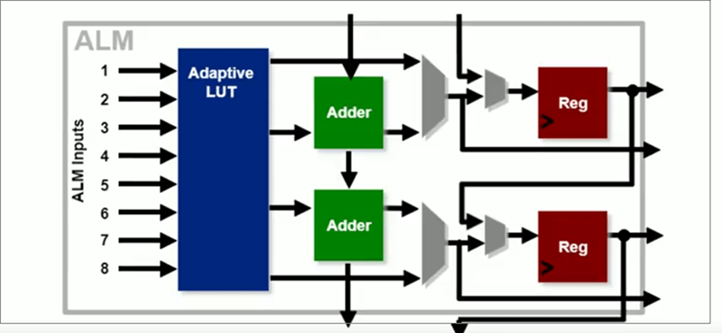
So what’s different in this video if you want to use another brand of FPGA? Some of the terms for things like logic elements and adaptive logic modules will have different names on different architectures. The particular architecture may be different, too because different FPGAs will have different flip-flop cells and special function blocks. This can also be different even among different FPGA families from the same vendor, especially when the vendor bought out some other company.
The information about why you want to use an FPGA, basic ideas about look up tables, clocking, and routing are going to be solid no matter what FPGA you wind up with. The general workflow description is useful, too, even though this can vary depending on the vendor and tools you choose to use.
On the other hand, Intel FPGAs are perfectly fine so we aren’t suggesting you take the training and absolutely go with something else. There are relatively affordable boards from most of the vendors and you’ll find that for all but the most complex projects the choice boils down to personal preference and, perhaps, price.
If you need a cheap Intel board, the MAX-1000 is about $30 and not a bad starter board. Our favorite starter board, though, might be the Lattice iCEstick which is dirt cheap and has an open source toolchain.


LEarning a MACRO HDL language like VHDL or Verilog really is a GATEway to LUTs of interesting things.
I wish there was some standard to convert between different manufacturers units like Gates, LEs, LUTs and Macros.
Now that Intel have bought Altera, are we going to see Intel FPGA chips with a “Altera Inside” logo?
here’s my problem, I understand the basics of it, have for a decade now, but someone make freaking tutorial on how to judge how much of an fpga do I need to buy. Its easy with micro’s, simple physical interface, maybe an 8 or 16 bit, needs some brains maybe a low end arm or a 32 bit model
FPGA’s phht, just choose one that you need, well thanks how do I do that (silence) its kind of hard to plop down the money on a dev board not knowing if its got the space of a half dozen PAL’s or so much space I could simulate an entire pdp11 with room to also squeak in a terminal
FPGA stuff aint cheap
It’s highly probable that if you don’t know how much do you need, you’ll be fine with the smallest of the recent offering, or probably a generation before that because the most recent ones tend to ditch QFP completely. E.g. take EP4CE6 as your starting point, create your project in Quartus and see if it fits with room to spare.
Good point. For many microcontroller projects, way more than you need is still cheap (for example: ESP8266, STM32F103 “Blue Pill”), so no worries about oversizing unless power consumption or physical size matter.
I usually find myself in one of two situations. 1) I have a board with a certain device on it and that’s what I’m using or 2) I have a device family in mind. I will start off small in simulation until I can’t stand it and then bump up to the next family member. Of course, I won’t always start with the smallest. I’ll make an educated guess. But by the time I’m ready to actually burn a configuration I should be about 95% there in simulation so I already know how full the device is. Keep in mind, too, that at high utilizations you may have trouble routing and making timing, so always good to not pack the device to 99.9%
Timing and area closure (fitting a design to the constraints of a given FPGA) is more of an art than a science for sure.
Only very experienced Hardware Definition Language (HDL) coders can estimate the size of a FPGA or CPLD needed just based on the mental concept.
In any case if you want to learn a HDL you need to focus on easy of use and learning.
Using your analogy with Micro-Controllers, you don’t want to start with a Micro that requires 200 lines of code for the configuration registers when you don’t know what most of them do.
In any case the chip you choose is far less important than how complex and difficult the learning experience is. After all your true objective is to learn a HDL rather than aim at a complex and specified project right from the start.
1)
First choose your HDL, Schematic Entry, VHDL or Verilog. Both the leading platforms – Xilinx and Altera support both VHDL and Verilog. I think they both also support schematic entry but I am not sure as I have never used schematic entry. In the US Verilog is most often used as company IP is often written in the older Verilog. However many code in VHDL and just plug in the IP in Verilog. Most of the rest of the world uses VHDL.
If you choose schematic entry then the largest circuit you will enter will be the size of a very-small to small CPLD. You will never use up even a small FPGA with schematic entry.
2)
Choose your IDE, In my opinion the Xilinx ISE platform is better for experienced users. However I would strongly recommend the Altera Quartus II WebPack for beginners. Once you learn one it is relatively easy to learn the other. A HDL is a HDL.
3)
Consider the cost of the programmer.
The Xilinx JTAG adaptor (which they call a Down Load Cable- DLC) is about $50
The Altera JTAG adaptor (often called a USB Blaster) can be found for $5 or less on ebay
Some boards have a inbuilt USB to serial bridge but I don’t recommend these boards as the software to drive them doesn’t fit in well with the IDE (if at all). Most boards with USB input however have a JTAG connector asw well.
4)
Decide if you want a all in one development board (which is often far more expensive) or if you are happy to have to have a breakout board and use flying leads or a bread board to make in IO interfaces yourself.
If you decide on an all in one board then one of your most important selection criteria will be any supporting tutorials specifically aimed at that board in the HDL you have chosen.
5)
Voltage considerations. Most all FPGA max out at 3.6V for a 3.3V chip. Newer FPGAs have even lower voltages like 1.8V This is an important consideration if you want to breadboard. Less so for a all in one board but consider that any IO breakout will have limitations. Native 5V CPLDs are all but dead – you will only find old stock. There are still some 5V tolerant CPLDs floating around but they are very small in gates.
6)
The size of the chip in Logic Elements (LEs), Macros, Look up Tables (LUTs), Gates or whatever is specified as the latest flavor by a specific manufacturer.
You mentioned Programmable Array Logic (PAL) which used a unit called a Macro. This is tiny tiny tiny by modern standards. For example I will go through some older CPLD chips from that way gone era.
From the PAL/GAL era
22v10 – 5V 10 Macros
More or less obsolete very small CPLDs
Xilinx XL9536XC – 5 Volt Tolerant 36 Macros
XL9572XC – 5 Volt Tolerant 72 Macros
Altera EPM240 – 5 Volt Tolerant* 240 LEs 180 Macros aprox
EPM570 5 Volt Tolerant* 570LEs 380 Macros aprox
*The spec sheet says to use series resistors for 5V tolerance but I never do and have never had trouble.
From the above you can see that there is APPROXIMATELY 3 LEs to 2 Macros.
A LE is basically a MACRO split in half and half of that macro can be used for combinational logic instead. This is why we don’t use the term Macros anymore.
Old and Small CPLDs that are mostly still in production or still kicking around on ebay breakout boards 3.3V
Altera Cyclone
EP1C3 – 2910 LEs
Altera Cyclone II
EP2C5 – 4608 LEs
And it’s all upwards from there even with CPLDs. Modern FPGAs are even still larger.
7)
Choose CPLD or FPGA.
From a learning HDL point of view the cheaper CPLDs are just the same in HDL but FPGAs do have features like Block RAM (BRAM). The amount of BRAM is usually small and its better to drive an external SRAM chip if you have the IO pins. If you have chosen an all in one board then choose external SRAM over SDRAM as driving a SDRAM chip is complex for a beginner.
8)
Choose a version of either Xilinx ISE or Altera Quatus II that supports the chip you have chosen. With each version upgrade they loose support for older chips so the latest version may not support the chip you have chosen.
9)
Now learn the HDL and IDE, code some chips
10)
Write your big project and synthesize it and see what chip it will fit into.
Buy the board you want now that you know how to choose the right one for you needs.
+1 Nice write up!
great stuff!
“ANOTHER INTRODUCTION TO FPGAS”
What an unfortunate acronym.
Yeah, it took me a moment to realize that “FPGAS” didn’t mean “FP Gas”.
AITF?
For those who don’t shy away from proprietary toolchains or the absolute dirtcheap, the Terasic DE10-Nano Kit and smaller Terasic DE0-Nano-Soc are relatively inexpensive, have decently sized FPGAs, and a ~1Ghz ARM HPS that can run any Yocto flavored Linux.
After you’ve dipped your toes in to the basics, https://bitlog.it/hardware/building-embedded-linux-for-the-terasic-de10-nano-and-other-cyclone-v-soc-fpgas/ is a real gem that covers the hardware design, HPS Linux image and cross-toolchain creation, and writing device drivers to marry the FPGA and HPS together.
As I mentioned in another article recently (FPGA Calculator) it’s odd when you combine a ~1GHz processor with a slow interface – like the Arduino connector on the DE10-Nano. Sure it increases the number of extras you can attach, but you’re not really able to make the best use of device speed.
The Xilinx based Red Pitaya has 2 ADC channels, and 2 DAC channels. If Intel / Altera / Terasic had a simpler version, with a single high-speed ADC and DAC channel (along with that lower speed Arduino interface), they could probably sell it cheaper. THAT would make an interesting kit.
People tell me – I’m dreaming. But it’s a nice dream.
The Terasic ADC-SoC has 2 150Mbps 14-bit ADCs, no high speed DACs though. There is a high speed 2xADC/2xDAC daughter board that comes in dual 20-pin GPIO that connect to any of the Terasic SoC boards mentioned. You’re definitely starting to push up your low end budget though.
Time to re-check the Terasic products. Especially that DAC daughter board. Thanks!
For 14-bit, I set my budget at US$310 – that’s the price for a 14-bit Red Pitaya through Mouser.
https://www.mouser.com/red-pitaya/_/N-1ynykvr/
Ah shucks *blushes*. I based it mostly off of the rocketboards guide and expanded the bits that were skimmed over :)
Friend, I think you have found your way to the wrong website.
Rather charming way of doing so, but still, feeding the troll I’m afraid ;-)
While I do find these things fascinating, as a hobbyist I have yet to come across a project idea that might possibly warrant using one. To me, FPGAs still seem as faraway as rocket boosters. Interesting and important for sure, but nothing I can make use of in my lab :-D
Fair enough! They really shine, at least at the hobbyist level, when doing simple manipulations on a lot of data real fast. So anything with video, graphics cards, SDR, etc. Actually it’s about the same for industry too. I just got back from a trade show where everyone was like “FPGAs for image processing”. But you’ve also got a lot of pins accessible in parallel, with very tight timings.
Of course you could just load up a soft microcontroller and have the CPU power of an Arduino with easy-to-overvolt IOs, no analog peripherals, no easy-to-follow code examples, and a daunting and opaque toolchain. Oh, wait, I see…
FPGAs: Good for what they’re good for!
A soft core can have much more power than an Arduino, at least for non-quark variants. 50-100Mhz is “trivial”, 300+ Mhz is possible even on relatively cheap FPGAs (hint: DSP blocks on Xilinx). Superscalar is possible, VLIW is possible.
FPGAs for experimental CPUs.
Unless you move the goalposts about how you measure CPU power. The FPGA will do more fixed-point MACs in a second than an Arduino can do in an hour. Need to run some CRCs? FPGA all the way. Really need floating-point? FPGA.
There are also many peripherals where the FPGA wins. Need 16 UARTS? How about 10 I2C modules? A dozen SPI hosts? Need a bunch of ΔΣ DACs instead of primitive PWMs? FPGA.
A popular application would be interfacing with complex hardware. For example if you build an expansion module for some old computer, you could do it oldschool with painful steamy 74xx, could bitbang with an micro that would be grossly overpowered for the job and still almost have no cycles to spare because of the timing requirements, or you could just FPGA it.
If you’re learning about DSP, it can be really helpful to set up FIR filters, IIR filters, etc. and actually SEE [or hear] the effect hey have on a signal. You can also “fiddle” with the factors that make up a filter, live, and see / hear the impact.
You can do this to some degree already with a PC and a sound card. FPGA’s combined with good IO can up the sample rate into the MHz, for better sample rates [or sampling higher frequency signals]
I’d naively hoped that when Intel bought into the FPGA game, that we might see another open source tool chain….
ah well….
What on earth could be the reason for such hopes? Intel, the famous company built entirely on principles of love, sharing and altruism.
I think the only thing Intel are notably open about are the drivers for their integrated graphics processors.
yeah nothing much there…. https://01.org/projects just cause they don’t shout about it, don’t mean they don’t understand it…
shoutout to your own guys making fpga boards: hackaday.io/project/25958-tinyfpga-a-series
On related note, any comments on the recent Cyclone 10 CYC1000 board https://shop.trenz-electronic.de/en/Products/Trenz-Electronic/CYC1000-Intel-Cyclone-10/ ?
25kLE with 8MB SDRAM looks like good deal for 30EUR, is there some catch?
Nice but still have the issue shared with most trenz board: no connectors references, so good luck to find what is where, there is no info on that in their design files.
Been bitten by this with icoboard…