The cool kids these days all seem to think we’re on the verge of an AI apocalypse, at least judging by all the virtual ink expended on various theories. But our putative AI overlords will have a hard time taking over the world without being able to build robotic legions to impose their will. That’s why this advance in 3D printing that can incorporate electronic circuits may be a little terrifying, at least to some.
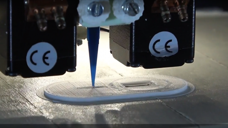
The basic idea that [Florens Wasserfall] and colleagues at the University of Hamburg have come up with is a 3D-printer with a few special modifications. One is a separate extruder than squirts a conductive silver-polymer ink, the other is a simple vacuum tip on the printer extruder for pick and place operations. The bed of the printer also has a tray for storing SMD parts and cameras for the pick-and-place to locate parts and orient them before placing them into the uncured conductive ink traces.
The key to making the hardware work together though is a toolchain that allows circuits to be integrated into the print. It starts with a schematic in Eagle, which joins with the CAD model of the part to be printed in a modified version of Slic3r, the open-source slicing package. Locations for SMD components are defined, traces are routed, and the hybrid printer builds the whole assembly at once. The video below shows it in action, and we’ve got to say it’s pretty slick.
Sure, it’s all academic for now, with simple blinky light circuits and the like. But team this up with something like these PCB motors, and you’ve got the makings of a robotic nightmare. Or not.
Thanks to [Simon Kühling] for the tip on this one.


This is dope but with costs dropping I can already see unscrupulous companies creating another environmental disaster by distributing promotional merch that will end up in the trash.
Kinda like those LCD screen/MP3 postcards
Has to drop quite a bit before it becomes competitive.
Ha you think we need 3d printers to have an environmental disaster? Hold my beer and watch this
Movie-plot threat: A bomb whose wiring can’t be seen because its entire circuit is enclosed in the 3d-printed enclosure, and it appears that there are complex metal traces throughout the plastic that could trigger the bomb if cut. Need to post this to Schneier.
That is what 3D x-ray tomography is for. Actually you could add that to the plot, smart cop 3D prints scanner to foil smart terrorist (yeah I know that is an oxymoron) who 3d prints bomb.
You could have also a couple x-ray radiation sensors that detonate the bomb if being scanned
Embed the device in the goop used to fill 1976-1987 Ford Duraspark II ignition modules. It’s sort of rubbery but pretty much impossible to cut.
Or on the other side, an intricate 3D printed circuit being used to make it difficult to physically break into a device that contains encryption keys or whatnot. (I recall Michael Harrison tore down part of a cash register that used a similar idea.)
Now I’m starting to think that 3D printing will be the next leap in disposable products evolution :(
I am sure injection molding will have that covered (pun intended), for the foreseeable future. ;)
Nah. 3d Printing isn’t cost-effective for anything other than prototypes and one-offs.
Very cool technology, as 3D circuit design could add simple options for smaller devices.
Maybe they can try direct printing on upside-down QFN, as stacking chips could be useful.
The downside of pure plastic circuit boards is increased stress/warping from temperature changes, so I doubt we will see even the terrible tolerances we get on FR4 anytime soon.
However, I really liked the idea of waterproof fastener free enclosures… maybe capacitive switches with the current tech is already possible.
This is very cool – I’m curious how they cure the conductive ink/epoxy. Is it heat? UV? Is there any affect on the plastic? Can the traces be printed over?
It’d be a lot of fun to try this…hey, what do y’all think would happen if you tried to extrude solder paste through a ~250C hotend?
That’s actually an interesting thought. What if you 3D printed ‘channels’ in the plastic and filled those up with molten solder?
That’d be a great way to set up deadbugging. Print a circuit with holes for the components, and use the mould as a holder that keeps the circuits in place while you solder.
It’s only slightly terrifying that you could have as many layers of circuits as you wanted. Soon we literally will be able to print brains.
Seems like the silicon is the (cost) limiting factor, not the layers on the board.
Now, if only conductive ink was actually conductive enough to be useful…
I love the printer.
I thought that the way it changed devices the it used is so cool.