There are at least two phases to learning about electronics. In the first phase, you learn about how components are supposed to work. In the second phase, you learn about how they really work. Wires have resistance and inductance. Adjacent wires have capacitance. Capacitors leak. Inductors have resistance. All of these things matter. [Learnelectronics] has a recent video that explores recovery time for a diode — a phase two conversation.
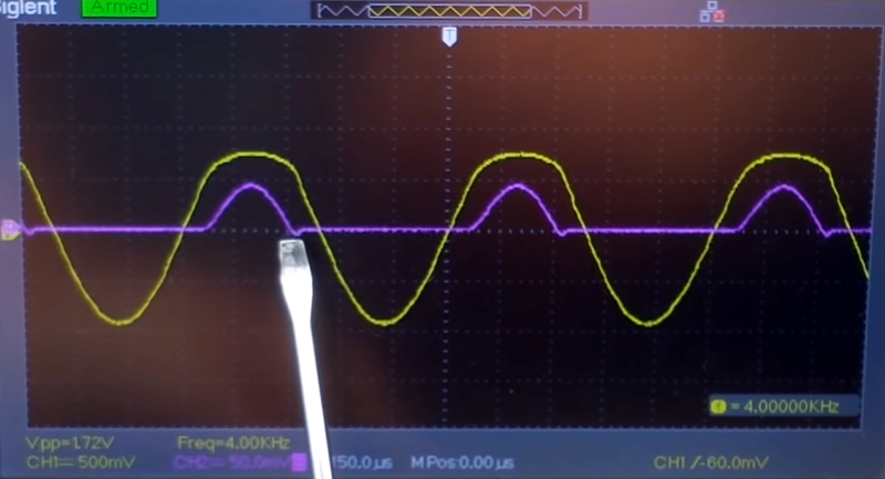
If you haven’t run into recovery time before, it is the amount of time the diode takes to shut off after it is conducting. This manifests itself as a little undershoot where the signal that the diode should block leaks through briefly.
The video looks at a few different diode types at different frequencies. The recovery time makes a difference in several designs including switching power supplies. If you dig into the physics, there is a usually a trade-off between several other parameters and recovery time. Just to give you an idea, the datasheet for a BAT42 Schottky diode says the reverse recovery time at 10mA is no more than 5 ns.
The video shows reverse recovery time, but forward recovery time is a thing too, though that usually isn’t such a big deal until you deal with very high currents. If you want a more technical explanation, there are good application notes from Vishay and Fairchild, to read.
If you want a different take on the same subject, [w2aew] also did a video on this topic a while back.


“There are at least two phases to learning about electronics. In the first phase, you learn about how components are supposed to work. In the second phase, you learn about how they really work.”
Third phase. Magic!
+1
the author knows what he talks about.
3rd Phase is Blue smoke evasion
Recovery time hack http://www.qrp.gr/technology/diodeaudioamp/Diamp.htm
Is that were the blues smoke comes into play?
I’d rather The Blues Brothers come in to play!
They’ll bring their own smokes.
For anyone interested in this particular subject I’d recommend w2aew’s excellent tutorial at https://www.youtube.com/watch?v=SBqLOrlA7QI . This guy is an excellent teacher (but not working as one) and always goes through the theory in easy-to-understand terms on paper first and then follow up with some practical demonstrations.
I highly recommend his youtube channel, it’s very nice and down to earth. No excessive talking and repeating like Dave’s eevblog, and no silly antics like electroboom, and not a speed-talker like “mikes electric stuff”
Yeah that is actually the last link in the post if you notice….
Third Phase: Magic Smoke…..
often accompanied by the phrase “I tought i understood it!”
Or the infamous “why is it doing that?”
Or “It worked before, it shouldn’t do that!”
“It must be a defective part, I’ll just replace it!”
My best story about this was when a bunch of physicists at an old job came to ask me to recommend a power transistor. They said they kept buying them at Radio Shack and they were “all bad.” So I asked what they meant by “all bad” and of course, none of them worked in their design. They were using it to switch current through some test ICs. Well, a lot of them. So the thing was doing a few amps total. I looked at their schematic and it looked OK to me. Very simple current mirror with an emitter resistor setting the current.
I asked them to show me the actual circuit. First thing I notice is that the emitter resistor is like a 10W wire wound resistor! So small changes in the emitter current (probably from Early effect) were causing huge voltage spikes and popping the BE junction on the transistor! The answer was to get a non-inductive wirewound resistor (they wind them one way and then the other way so it cancels out).
Now granted, we were in the business of dealing with failed semiconductors. So I guess if that was your only job you could get the idea that all devices just fail all the time. But it was amazing to me that several people who had physics degrees — probably one or two pHd’s in the mix — just thought Radio Shack had sold them a dozen bad transistors and couldn’t conceptualize that maybe it was their own fault.
“It worked in simulation!”
Yes…And then I noticed, I forgot the heatsink of the PSU, for which I designed a fan control, was not potential free. But after repairing a blown trace and replacing some low value resistors it worked very nice.
Unfortunately you normally do not include heatsinks into a simulation. :-)
Generally speaking there are three models for components.
The ideal model, where the diode conducts in one direction only.
The first approximation, where obvious factors like 0.7v forward voltage drop are estimated in the design.
The second approximation where most factors such as impedance and recovery time are taken into consideration.
Most hobbyists can get along fine with the first approximation for most projects. Engineers or those working on complex projects that involve RF will have to delve a lot deeper into the specs of each component.
Unfortunately this is one of those times when someone on the internet has good intentions but puts out misinformation.
Note how the output goes negative while the input is still positive. This only happens with capacitance. If the recovery time was at fault, the output wouldn’t go negative until ~0.7V after the input went negative.
ALL ‘dips’ in the video are due to capacitance in his setup. The capacitance of the parts, breadboard, probe etc. Some of it is due to the inductance as well, but mostly capacitance.
His part recommendations are also incorrect. Reference the Youtube comments for correct information…Can’t believe I just typed that.
Surprised HaD deleted my last two attempts at posting this.