We are spoiled these days because you can shop online and get all manner of inexpensive electronic goodies shipped to your door. This is due to the fantastic electronic fabrication workflow that has grown into a global powerhouse, facilitated by complex yet inexpensive integrated circuits! But it took a few intermediate steps to get here, and one of those is known as a couplate.
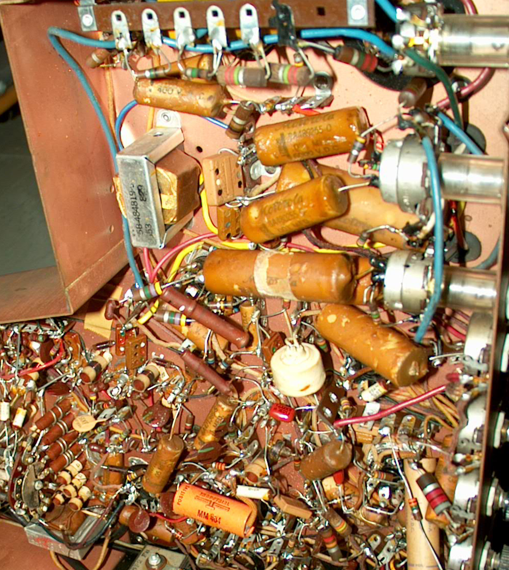
When I was a kid, the big deal was to find an old radio in the trash. You could spend a few hours stripping all sorts of parts from the thing and add it to your collection for a future project. Of course, old radios from the 1970s and earlier had a lot of the usual parts we use today, even though many of them were bigger — no surface mount parts yet. Since older radios were the usual find in a dumpster, tubes were common but you could find some transistor radios.
Once in a while something older. There would be a little box with some wires poking hiding in an old radio from the 1940s or 1950s (too early for ICs). In a way, though, these were predecessors to the Integrated Circuit and they went by a few names, depending on who sold them. PEC (Printed Electronic Circuit), a couplate, or a BulPlate, are all names for hardware that was a stepping stone between discrete circuitry and ICs.
Collections of Passive Components
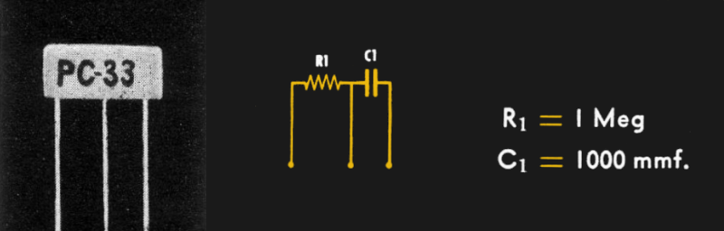
PECs were most common in tube sets and they didn’t have any active circuitry. They sere often set up to handle audio filtering or some other common task using just resistors and capacitors. Companies known for these devices Areovox (PEC), Centralab (couplate), or Sprague (BulPlates). The example shown here, the PC-33 from Centralab, sold for fifty cents and had three terminals
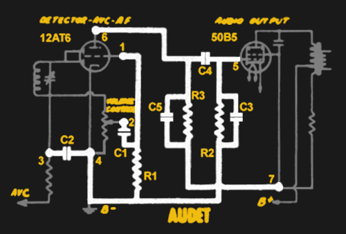 The PC-33 is not terribly impressive, but a PC-151 (see right) had 7 pins and the schematic is quite impressive. The couplate itself only had the bold components, not the tubes and other components showed in gray. That little jewel cost about $1.15. Doesn’t sound like much, but in 1950 terms that was like $12 today. In fact, we found one on eBay for $11.90 so maybe there’s something to that.
Another place you would find these were in TVs where a vertical integrator PEC could help with sweeping the CRT. It was basically three resistors and three capacitors set up to help generate a vertical deflection ramp.
Active Devices
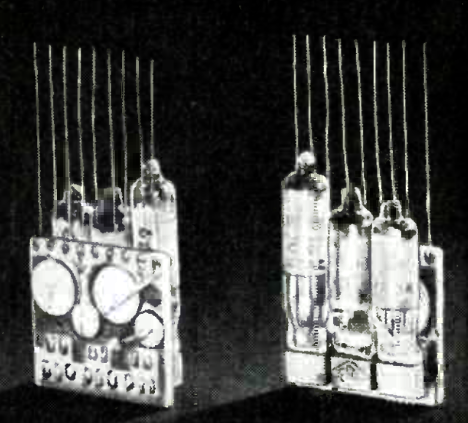 There were a very few PECs made with tubes as active devices. Well, more accurately, with tube sockets. Some 1950 promotional material from Centralab said:
There’s never been an electronic device like Centralab’s Ampec. It is one compact unit permanently bonded to a master plate with all components of an audio amplifier — tube sockets, capacitors, resistors, wiring. It’s a full three tube three stage speech amplifier.
Centralab Ampecs are widely used in hearing aids, for the most trouble-free performance ever attained. Ampec has other interesting applications, as mike pre-amplifier, etc.
The module — without tubes — was an inch and a quarter wide and nearly as long. An Allied Radio catalog described it as “no larger than a book of paper matches” and sold it for $15.29, including the tubes.
Construction
The American Radio History site has so many old magazines and catalogs and, as usual, it didn’t let us down when looking for more information about these old components. The December 1949 issue of Radio and Television News (PDF) has the start of a two-part article entitled “Printed Circuits.” The cover with the smiling housewife, beaming at her brand new intercom while her five inch TV set perches next to the sink is priceless, too.
According to the article, Centralab began mass producing printed circuit boards in 1945 for a mortar shell proximity fuse. But these were not printed circuits in the sense that we think of them today. A ceramic substrate was the base for silver and graphite paint applied via silk screen. The silver makes wires and the graphite makes resistors. Seems like conductive ink circuits isn’t at all new concept!
The ceramic was fired in an oven and capacitors were attached. In some cases, conductive paint on both sides of the ceramic would form capacitors, too. Of course, small flat inductors were also possible. Supposedly, inductors could be covered with an insulator and painted with ferrite paint to increase inductance, but that doesn’t sound like it would get you very far. In more modern times, this same basic technique is how you make hybrid thick film circuits, not uncommon in high-reliability applications.
The author notes that you can use other methods such as rubber stamping or lithography to ink the printed circuit board. There was even talk of using decalcomania which is exactly what it sounds like, but I still had to look it up. There were many other methods that didn’t catch on over the long term. For example, “dusting” had metallic dust spread on a substrate and sintered in place much like some metal 3D printing processes. We were especially amused by the cylindrical boards that built circuits around a glass tube.
Build Up and Teardown
The second part of the article (PDF) covers creating your own printed circuits using conductive and resistive paint from DuPont. Since DuPont wasn’t going to sell you a few ounces of these paints, an enterprising Michigan company was selling smaller quantities and kits. You had to find your own substrate and we find it amusing that they suggested using an asbestos board.
 A Russian site has a great teardown of an old tape machine that used modules like these. The tape player may look bulky by today’s standards with its large battery and tubes. However, for its day it was quite svelte and cheaper to manufacture thanks to the couplate technology.
It is hard to remember a time when consumer electronics were wired by hand with real wires. We’ve all seen computer backplanes that looked like plates of spaghetti. Printed circuit boards would change the face of electronics forever. Integrated circuit modules, even more. A look at the very early birth of these technologies is sobering when you realize all this was less than 100 years ago.
These methods didn’t last long. By 1969, boards were a bit more like we think of them, although there was still a ways to go. You might enjoy the Tektronix video talking about those kinds of boards, below. And it’s also worth a mention that one of most mesmerizing component assembly periods is tinkertoy and cordwood construction.


One of the earlier examples of this is probably that 1940-ies radio where resistors, capacitors & inductors are directly printed / etched on some pcb like (ceramic?) subtrate.
The B&W video of that radio is an amazing example of automated production from a time that must have been very futuristic (and probably too expensive).
Search youtube for:
ECME – electronics automated production 1940’s style!
Automotive as well.
These always left me cold on the value of the item and it’s fixable worth. Trouble in a cookie.
Right. Usually, these were generally product-specific, so good luck finding replacement parts. Furthermore, schematics wouldn’t show the contents of the modules, and if they did, these didn’t contain component values, so good luck replacing a module with individual components.
A successor to the PEC were the Hybrid modules and Thick Film techniques, with direct printing of resistors and capacitors, these got out accelerated by the IC industry. They have some niche uses still.
I would say they are ripe for a revival as a hobbyist technique, given we’ve seen here recently laser sintering of conductive compounds, and I’m thinking 3D printed circuit board fabrication is not going to play nice with conventional soldering methods. It also does not leverage the 3D part much. Some hybrid of precise laser sintering of thick film like 3D printer deposited materials might offer a revolution in table top, smaller than surface mount + PCB but still not as compact as single IC fabrication possibilities.
My 1970’s-era 100-in-one project kit from Radio Shack had a component called “integrated circuit” which was more like this than a real IC, with apparently printed resistors and some discrete components bonded to what looked like a ceramic substrate and covered with transparent polymer. I always wondered what gave them the idea to include that oddity.
Because it was the future.
An don’t forget the LOEWE multi-valves from the 1920ies …
“The device consisted of three triode valves (tubes) in a single glass envelope together with two fixed capacitors and four fixed resistors required to make a complete radio receiver. ”
https://en.wikipedia.org/wiki/Loewe_3NF
So essentially, you’re saying that the integrated circuit predates the transistor.
That depends on the definition of “integrated circuit” ;-) But it was a very interesting piece of hardware, almost a century ago. I think the basic idea of an “IC” already existed before there were semiconductors – it was just natural.
Regarding the definition of “integrated circuit”, the defining advance that created integrated circuits out of silicon was applying the same techniques used for making individual transistors, to make multiple transistors on a common wafer, and additionally making passive components using mostly the same technology to provide biasing and coupling functions. In the same way, if you want to make an integrated circuit with vacuum tubes, the way to do this would be to use vacuum tube manufacturing techniques (glass rods, metal wires and sheets, spot-welded together, and encasing the whole thing in a glass envelope) to include passive bias and coupling components spot-welded in as well. I assume that these Loewe tubes did essentially that, so I would call that an integrated circuit.
Semiconductors, like rocks, have always existed. The first semiconductor crystal radio was in 1904.
I’ve seen the Tektronix film before, and it’s very helpful, in that it describes how to make a double-sided PCB with plated through holes, using technology available in the 60s. This has been the holy grail of DIY PCB makers since forever. The two critical steps appear to be 1) using an electroless copper plating process to get the initial few microinches of copper onto the insides of the holes, onto which conventional plating can be applied, and 2) the process of first electroplating the traces with copper, then gold, then removing the resist and etching the remaining copper, leaving the copper that was protected by the gold. In the film, they say (twice) that some other metals can be used instead of gold.
So I have two questions: 1) anybody know a simple (i.e., not very difficult, expensive, or dangerous) process for electroless copper plating onto glass-epoxy?, and 2) Since I already have a big bottle of electroless tin solution that plates onto copper, is there an etchant that will eat copper but not tin?
P.S., all of the kits and YouTube DIY videos I’ve seen for plating onto non-metallic surfaces seem to involve first coating the surface with something at least slightly conductive, then electroplating onto that. I’m trying to avoid that approach since there is then an issue about how to get a good connection (mechanical as well as electrical) between the through-hole plating and the surface pads.
Something like graphite spray wouldn’t work? https://uk.farnell.com/kontakt-chemie/graphit-33-200ml/coating-conductive-200ml/dp/832959
I know about a commercial PCB process which uses tin instead of the gold. I think it’s called metal-resist process. So, yes that works.
Several days ago I saw a very good video about electroless copper plating in youtube. The guy made dozens of experiments, basically to make copper traces on 3D printed parts.
The recipe for the copper solution contained:
CuSO4
NaOH
NaCO3
sodium-potassium tartrate (cream of tartar?)
formaldehyde
I do not remember the quantities, but I think you will find the video.
The catalyst for the activation of the surface was palladium based:
Palladium chloride
tin chloride
The chemicals are corrosive, but not “extremely dangerous”. The drawback of this chemicals is, that they have a bad shelf life. They are quite unstable, because that is part of their principle of function.
Many of the experiments in the video were about selectively activating the surface of the substrate with a CO2 laser to selectively deposit the metal.
So this is where Morgan Freeman got his voice acting skills from.
A tube based hearing aid!! I can’t stop imagining somebody in the 40s with glowing tubes sticking out of their ears, lol. In retrospect it’s obvious that hearing aids must have existed before they were small enough to fit in your ear but for some reason I never thought about it before now, and now that’s all I can see. :)
Not so different from the bluetooth earpiece with the glowing blue LED.
But a blue LED is (and looks) much cooler than a tube. :-)
For awhile I had a castoff tube-based hearing aid amplifier. It was about the size of a cigarette pack and connected to the actual ear transducer by a wire. It had IIRC three micro-miniature tubes I still have a few of those tubes, about 3/8 inch diameter with a linear row of wire contacts from the bottom pinch.
Isn’t it similar to e.g. resistor ladder in single case? Not sure how it’s called properly