It is widely accepted that Gutenberg’s printing press revolutionized thought in Europe and transformed the Western world. Prior to the printing press, books were rare and expensive and not generally accessible. Printing made all types of written material inexpensive and plentiful. You may not think about it, but printing–or, at least, printing-like processes–revolutionized electronics just as much.
In particular, the way electronics are built and the components we use have changed a lot since the early 1900s when the vacuum tube made amplification possible. Of course, the components themselves are different. Outside of some specialty and enthusiast items, we don’t use many tubes anymore. But even more dramatic has been how we build and package devices. Just like books, the key to lowering cost and raising availability is mass production. But mass producing electronic devices wasn’t always as easy as it is today.
Pre PCB
 At one time, electronics were assembled by hand with point-to-point wiring and a variety of terminal strips and connections (for example, see the 1948 Motorola TV set to the right). Wires formed connections to the terminal strip (the component with five lugs near the top left), sockets, lugs on controls, and components.
This is in stark contrast to today where all the components would mount on a printed circuit board (PCB). Actually, PCBs in some form have been around since the early part of the 20th century. Even [Thomas Edison] tried to plate conductors on paper.
Despite some limited use, PCBs didn’t really take off until World War II. German mines and U. S. proximity fuses used them. Still, it would be well into the 1950s, though, before consumer electronics started to really use PCBs.
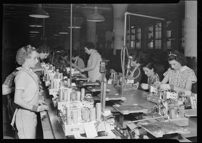
There are some technical advantages (and disadvantages) to using PCBs. But the most obvious advantage is just in labor savings. Assemblers used to use photographs and checklists to be sure they made every required connection. Not only was this labor-intensive, but it was also prone to error. The photo below shows an RCA radio factory in 1937.
Despite the name, printed circuit boards are not always printed (in fact, today, they are rarely printed). But the idea that you can make one template and automatically make tens, hundreds, or thousands of identical copies is the same idea of the printing press.
Pre IC
The other printing-like process that changed electronics forever was the integrated circuit. While the PCB allowed wires to be reproduced flawlessly, the IC lets you create entire circuits with many components and then reproduce them relatively easily. There are other advantages, too (miniaturization, close matching of active devices, etc.). But the ability to produce a CPU, for example, with all its components and wiring repeatedly using a reasonably simple process has driven price and innovation in the electronics business since it became available.
If you think about it, the IC makes a lot of things practical. Let’s say you are going to create a fish finder that uses a sonic pulse to find your dinner (or the bottom of the lake). You probably need an instrumentation amplifier. How much could you spend to develop it? You probably can’t sell millions of fish finders, so you won’t have a lot of time to refine your design. It probably can’t have too many components in it either, or the price will go up and you’ll have even fewer sales.
You can buy an instrumentation amplifier as an IC very inexpensively. The company that makes it probably spent years getting it to the current state that it is in, going through multiple product iterations. Although more components do drive up the cost of an IC (due to driving up the die size), it doesn’t raise it very much, especially at smaller die sizes where manufacturing processes have very high yields. So your choice is to design your own inferior amp using a few devices at great cost or spend the buck or less to get a well-tested design with dozens of devices and great specifications. Easy choice. Of course, if you can find a highly-integrated fish finder IC (don’t laugh, the LM1812 was a thing; see page 81 of this old Popular Electronics) then you can use that and be done with your whole design in an afternoon.
Better Living Through Military
The military is often the first to find ways to pay for new technology. They had been searching for a reasonable way to get more reproducible electronic assembly for some time. The U.S. Navy, for example, had project Tinkertoy. The idea was to make little modules out of ceramic with silver patterns painted on them. Components like resistors and capacitors could also be placed on the boards using automated processes. At the end, modules stacked together and little tabs around the edges served as a guide for interconnection wires as well as keys for orienting the boards.
You can see a very detailed–and a little stiff–video from 1953, below, explaining how the system worked. NIST (the technical muscle behind Tinkertoy) also has a photo gallery of both the devices and the pilot plant.
https://www.youtube.com/watch?v=DhuuOWteelc
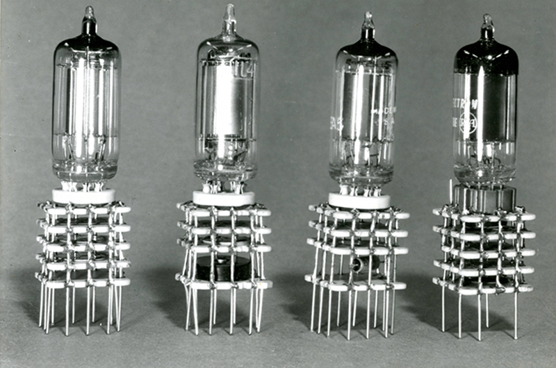
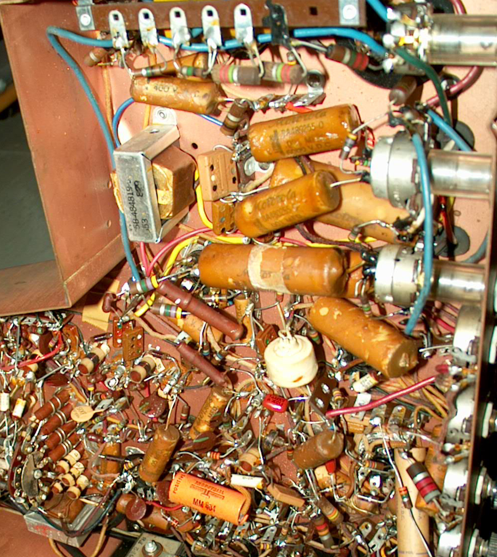
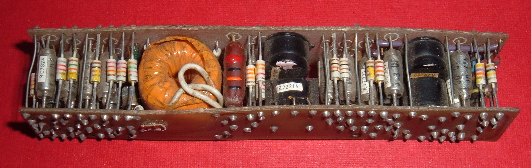
Cordwood
This was an improvement, of sorts, over another technique often used in military electronics back then known as the cordwood module. Cordwood modules were the ultimate in packaging density and shock resistance when using normal components and found use in military, space, and high-speed computer systems (since the density allowed wiring to be shorter).
The idea was to use two insulating cards. Components like resistors would bridge between the two boards and nickel ribbon would form wiring on the outer surfaces of the insulating cards. Thinner cards were used where ribbons intersected. Later, single sided PCBs would sometimes act as the cards and copper traces replaced the nickel ribbons. The module in the picture below uses this method.
Of course, if a component in the middle of the module went bad, you had a lot of work to get to it.
Don’t Forget the Army
The Navy wasn’t the only one thinking about this. The Army had their MM (Micro-Module) concept that looked a lot like Tinkertoy. The document covered late 1962 which was the 19th quarter of the program, so it was a little bit behind Tinkertoy. The MicroPac computer used as a test case looked pretty interesting and surprisingly compact for its day.
There were probably other module standards floating around (The NSA’s “flyball modules” come to mind), but really what everyone wanted was the integrated circuit. Then again, the first IC was in 1960, so the Micro-Module and its siblings were doomed almost from the start.
Modern Times
Once in a while, you’ll still see something done in the cordwood style (like the blinking light board in the video below). The board in the video is actually sold as a kit with no instructions as a puzzle challenge. Your job is to build it without looking at instructions (like we would do that, anyway).
Of course, you still see standardized modules around. It is just usually, they take the form factor of an IC. The Basic Stamp comes to mind. You can get whole ARM systems on a little DIP board. There are still a few places where hybrid integrated circuits are used instead of pure integrated circuits.
The Time Has Come
It is interesting that looking back you can see the pattern. The industry clearly wanted cheap standardized modules that didn’t require a lot of hand assembly. Just as the printing press allowed mass production of books and other reading material, PCBs allowed mass production of wiring and ICs the mass production of entire circuit “boards” with components.
There are more modern examples, too. Everyone was moving towards small boards that could run Linux when things like the Gumstix and the BeagleBone appeared. But the Raspberry Pi made it cheap and that’s what pushed high adoption rates. We are already seeing those get pushed into the chip level, too.
What you have to wonder is what trends are we in the middle of today? Will someone come out with a cheap multimaterial 3D printer (that includes metal or circuit components)? We are pushing to where the whole planet will be bathed in wireless networking, but at great cost. Will a Hackday author in the year 2110 write an article about how we used to build cell towers and satellites everywhere to get network devices connected? Spotting those trends can be lucrative or–if you fail to act on them–frustrating.
Cordwood module photo by [ArnoldReinhold] CC BY 2.5


My researching of Tinkertoy turned up an interesting irony, some of the best sources of information about Tinkertoy were Russian.
There are a number of significant electronic packaging techolongies that weren’t mentioned. Here are a few that went “mainstream”:
Vacuum tube “ICs”: Just like transistors, vacuum tubes were designed that put many devices in the same bottle. First twin triodes, then triple triodes, and a whole succession of increasing complexity. Today’s vacuum fluorescent displays are actually hundreds or even thousands of individual triodes; one per pixel.
Thin-film: Used for resistor networks, and other passive “ICs”. Resistive traces are deposited on a ceramic substrate. Capacitors have also been made this way.
Chip-On-Board: The raw unpackaged semiconductor (diode, transistor, or IC) is bonded to a PC board, and covered with a blob of sealant. You’ll see this used in millions of consumer products.
CoB was a lot later–at least from my exposure to it. Thin film held on for a long time and there’s still some of it around. Actually, that could be a good retro about the evolution of tubes. There were a lot of innovation there at the end. Acorn tubes, nonodes, Those cute little nuvistors (I used to have some; not sure where they are now).
Compactron! Lotsa pins for each tube section. 11 or 12 I forget.
CoB was something I’ve seen in a lot of watches due to the small space. Thin-film when I use to work with microwaves. Funny thing about vacuum tubes is there may be a comeback (http://newatlas.com/nasa-vacuum-channel-transistor/22626/).
I love the way the Tinkertoy film dances around the phrase “proximity fuse” which is obviously the product that justified building the pilot plant.
They device they showed was not a proximity fuse. My guess it was the guidance section of a sidewinder missile or a sonarbuoy. By the time of this film proximity fuses where a decade old.
Here’s another one – ECME
https://www.youtube.com/watch?v=3QHizDkrFqg
these robots are Taking Our JOBS!!
http://i.imgur.com/K71PiAI.jpg
I’ve been making character ROMs for a Kerbal Space Program controller using the hoards of diodes I have on a reel that I got for free. I kinda like some of the retro techniques. The one on the left is my fourth ROM module. It’s to display labels for each display to show either the distance units in various scales of SI units (m, Km, Mm, Gm, up to Ym), ∆V, –, and an all segments test character.
That looks great!
Thanks! Each one tends to be about and afternoon’s work, and as the picture clearly shows, I’m getting better with each one! Here it is in operation.
http://i.imgur.com/V3Pkbp5.gifv
Yowza! Nicely done :)
“No, I will not fix your radio”
“Cordwood” or “Stacked” prototyping (and even in production at a smaller scale) works great. Stacking stages that dissipate heat is a good example. You can separate layers so air-flow (especially forced air-flow) is effective compared with planar designs. The real experts in SMPS design use this often. Breakout the SMT part with a lot of heatsinking and it becomes a “part” than can be stacked with the low-power side components.
I’ve done repairs before, where a part damaged the PC board. I’d just stack the replacement over the damaged area and bypass the mess. Likewise though, if I see damage in one area, I might make the same mod to all similar areas, to prevent future board damage if another circuit blows. And indeed, you are correct about airflow.
I find electronics from that era fascinating maybe because everything I grew up with already was PCBs and ICs.
See how the Olivetti Programma 101 does Cordwood:
//embedr.flickr.com/assets/client-code.js
and
//embedr.flickr.com/assets/client-code.js
no preview, so here goes nothing…
indeed nothing. next try:
https://flic.kr/p/pwSVPx
and
https://flic.kr/p/pwSUGT
Olivetti made some pretty machines, inside AND out! :D
Regarding cordwood… “Of course, if a component in the middle of the module went bad, you had a lot of work to get to it.”
I’m catching up, reading through recent HaD articles a bit out of order. Anyway, this makes me think of the recent article about desoldering pins. That might be just the trick to remove a single component. I suppose putting in the replacement is still quite difficult without desoldering the whole thing.
I built a number of very small 12 to 24 volt converters for operating 24 relays in a 70 mh transverse amplifier to make the unit very small I made a tinkertoy module using a uc3842 and it works great I built xmas light flasher using home made tinkertoy module as well
Original tinker toy video is available at
https://ia802803.us.archive.org/28/items/Jeff_Quitney_me/20161129-Project%20Tinkertoy%20%28IC%20Precursor%29%201953%20US%20Navy%3B%20Automated%20Manufacturing%20of%20Modular%20Electronics.mp4
it was killed from youtube