The first thing you probably asked yourself when learning how to lay out PCBs was “can’t the computer do this?” which inevitably led to the phrase “never trust the autorouter!”. Even if it hooks up a few traces the result will probably be strange to human eyes; not a design you’d want to use.
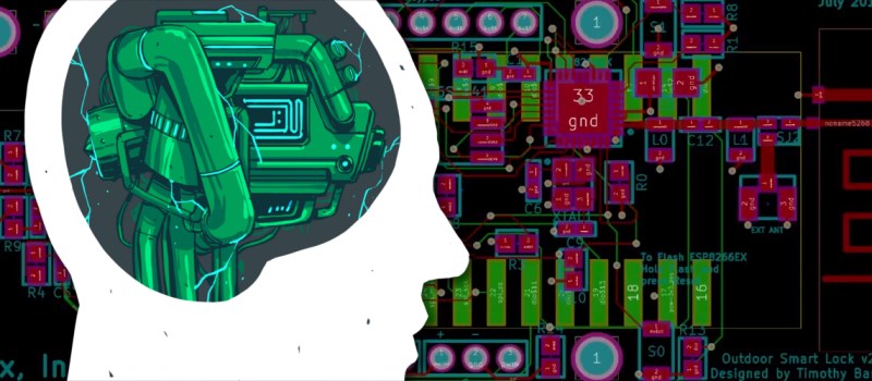
But what if the autorouter was better? What if it was so far removed from the autorouter you know that it was something else? That’s the technology that JITX provides. JITX is a company that has developed new tools that can translate a coarse textual specification of a board to KiCAD outputs autonomously.
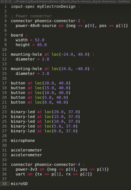
How do you use JITX? At this point the company provides a front end to their tools; you use their website contact form to talk to a human (we assume) about what you want to make and how. But watching their demo videos (see the bottom of this post) gives a hint about how the tooling actually works. In brief; it takes a specification in a domain specific language that describes the components to use, then compiles (synthesizes?) that into KiCAD files that can be sent to fab.
Removing the Human from the Equation
What level of abstraction does JITX work at? If it was an autorouter you’d select components and do some floor planning to place components before hitting the go button and getting a coffee, maybe even lay down some of the more complex tracks. That is to say, there is no abstraction at all. JITX can operate at a much higher level. You can specify which parts go exactly where and use it as an autorouter but where the tool shines is when the human specifies less, not more. The user can plug in specific components, board outlines and the like. But they can also just say “micro USB connector” and “Teensy 3.6” and JITX will figure out what connects where, place components, lay out tracks, and crop to a board outline.
But it can go even higher level than that. [Duncan] the founder and CEO told IEEE that you can “request a board with BLE and a microphone” and the tool can do everything else. It will select parts, figure out support infrastructure like power supplies, place the components, route the board, and emit design files. That’s damn near the entire design from napkin to product, which incidentally is a service JITX offers.
Control Freak v Push Button Designs
So the next question is who is this for? We have electrical engineers who may feel somewhat displaced by a technology that replaces large parts of their workflow. Even if they used it, do they effectively become programmers? Or HDL-authors (nowadays engineers who write HDL would be working on FPGAs or similar)? One could imagine an EE using a tool like JITX to augment their process by designing the totally bone-headed parts of a project which require no creativity. We’re not sure JITX would agree, but the not-groundbreaking-design market seems pretty large; enormous in fact. Especially when you consider that it includes entire products that are unsexy to an engineer but still need to be created. It might even include empowering people and organizations who would not have considered making hardware before.
Anyway, what does that market look like? Let’s consider a few examples:
- There’s often a need to make little bits of connective tissue in the form of simple boards with funky connectors to adapt between arbitrary connectors. A tool that could take, for instance, DigiKey part numbers and excrete design files for production could be a nice streamline. The end game here might be getting the board fabbed and assembled too, so the process would be completely turn key. Though such a product would need to be extremely fast or it might only be useful for nasty fine pitch connectors which are hard to prototype by hand.
- The firmware engineer who needs a test board made. Some firmware engineers do the electrical CAD to make a board themselves, but early prototypes are usually constructed by bolting together development boards. This is a great solution! But if a tool existed that effectively did the same thing but output a PCB instead we could imagine it finding traction.
- The largest and most terrifying market might be the Generic IoT Device. How many times does an EE really need to design something with a modularized nRF52, pick-your-favorite-sensor, and a coin cell? If JITX could generate form-factor designs with common “generic” devices like this it would probably be a huge leg up for a certain class of simple product.
Looking at theJITX website, they actually offer all of these in a pretty interesting fixed pricing model. Interconnect boards are “Adapters” and are a set at $499 a design given certain constraints. They also offer to design entire PCBAs below a certain complexity in 24 hours and at a constant $3,000. It sounds like a napkin sketch is all that’s required to make a board.
We’re pretty excited about what the future holds for more intelligent design tools! Tell us what you think you might use a tool like JITX for (or not!) in the comments.
Check out this demo video which includes a literal napkin sketch. It includes some description of the DSL used to specify the board (an expanse of FR4 to connect a bunch of dev boards together). They move on to specifying the parts instead of breakouts and use the tool to redesign the board at that granularity.


So, this is a hack-vertisement. Can Hackaday please not stoop so low as to have ‘native advertising’ like so many sites are doing these days?
Well said!
+1
I understand the sentiment and agree with it. This is not a paid article, Hackaday doesn’t publish sponsored articles. The tool was interesting to the author and he presented it with the excitement he felt at the prospect of it being something different. I did find Nate B’s comment below to be a good one. Articles like this would benefit from more comparison with similar services and we’ll keep that in mind when working in these in the future.
Yeah, this is really cool. Even if it is advertising, it fits into the general genre. Keep it up. Hackaday continues to rock.
Could also have mentioned https://sourceforge.net/p/phdl/wiki/Home and https://electron-lang.org which are open source attempts at DSLs for circuit description. There are more interesting projects in that space including Skidl which has been covered here before.
When the article starts with “The first thing you probably asked yourself when learning how to lay out PCBs was “can’t the computer do this?” “… it makes me feel old.
Because when I drawn my first PCB I used a bare piece PCB and drew on it using a magic marker (which worked surprisingly well). The second time I drew a PCB was with an ink-pen and a piece of transparent paper (great, now I had to draw the lines only once but I could make many PCB’s and they would all be the same).
It was only years later when I finally got to computers being able to draw a decent PCB. Because autorouters on simple PC’s in combination with cheap PCB software that simply wasn’t ready for serious routing of PCBs (it created 100’s of unwanted vias and it never completed). This combined with my youthful ignorance and arrogance made me decide I could do it better on my own.
Thankfully many of the problems (technically and mentally) were slightly solved by the decades that followed.
Yeh. Use to use premade puppets, a sheet with a grid, and rolls of line tape in various widths.
:o)
Joking aside, “can’t a computer do this?” is a perfectly justified question because of the complexity increase over time, IMO.
It’s doable to stick adhesive tape on a PCB in order to route a few 2…20 pins parts, but insane do try the same for a 2000+ Intel LGA pinout, where traces are almost invisible, and the number of layers sometimes are so many that they make the PCB sandwich thicker than a banana plug.
I have a lot of trouble with routing PCBs, it’s just not something that comes to me easy. It would be nice if I could just indicate roughly that, say, I want this or that component near the edge of the PCB, I want these components roughly grouped together, I want so and so much space between the components so that I can solder the board without needing a pick-and-place machine, and let an autorouter go wild and produce the board.
For me routing PCBs is a form of relaxation- I look at it like a maze which makes it like a game to get all the pins connected the right way with out crossing over. ( I etch my own pcbs so try and stick to on e layer)
It doesn’t mean I make make fantastic layouts but I enjoy doing it.
I call bullshit. The gate example is stupid – the whole point of a breadboard is that you can make changes easily, and get soething running quickly, without having to wait for a PCB.
I’m pretty sure this a paid article considering that the website says $3K for them to design a board with active components or a mere $499 for the to design an adapter board with up to 5 connectors.
KiCAD’S FreeRouting isn’t all that bad. My very first design was for a product I am building. The design is a small RPi I/O board with EEPROM, I2C ports, serial port, TVS diodes, LED driver, USB power, fuse, MOSFETs, switches, and the usual caps/resistors/diodes… not advanced, but definitely a few steps above beginner. I autorouted the thing and tweaked it only a little, improving trace widths and such. Handed it to an experienced radio engineer to QA it before FCC testing and he said “Not bad for your first board.” :-) He only had a few small suggestions. Seems to me FreeRouting can be a good foundation for further improvement.
A single human will still do these cheaper and faster than their turnaround times. I’d love to see an AI service that can do it instantly and perfectly for cheap, but without these actual benefits what’s the point. The examples look very organized, but very simple. Boards with that much space can easily be routed even by beginners. I want to see the real complex stuff, the stuff that would take a human weeks, then it would be worth paying for it.
When I read the article, I was kind of wondering if this really is an AI behind this, or if the website just takes the mark-up for a product, makes a preliminary board layout, and send it to a real live EE who draws up the board for you. They’ve certainly priced it high enough to turn a decent profit even if that is what they’re doing at the back end.
Yeah, this reeks of Mechanical Turk. That or a very small list of predefined parts and some scripts to run KiCad’s autorouter.
You guys are so cynical. Mechanical Turk. Sheesh. AI can do this stuff today already. Soon, it will be free. Just a matter of time. Remember how much SDKs used to cost? Free.
“But they can also just say “micro USB connector” and “Teensy 3.6” and JITX will figure out what connects where, place components, lay out tracks, and crop to a board”
I imagine with enough information yeah it can. Everything from complete parts descriptions, to international standards.
This leaves a lot of questions about who’s responsible for troubleshooting when things don’t work.
One company says it’s a revolution. Sure, they wanna make money and make the world their slave. Sorry I’ve gotten too cynical. Seems more like a paid adversion where they can outsource their work to the paying customer. Their script still need a input from a humanure.
PCB routing is very similar of the TSP: https://en.wikipedia.org/wiki/Travelling_salesman_problem
It’s an openended question, with movable parts and traces. How can we choose the BEST
path and places?
It’s even worse than the TSP. We have some good polynomial approximations for the euclidean planar TSP. Autorouting is closer to the Steiner Tree problem: https://en.wikipedia.org/wiki/Steiner_tree_problem
You don’t need the best, just “good enough”
It might be interesting to throw GPU power at the routing problem,and some AI might be useful to point it in the right direction.
However the biggest factor to getting good routing is placement – tools that can assist with this would likely be at least as useful as autorouting.
> You don’t need the best, just “good enough”
> It might be interesting to throw GPU power at the routing problem,
Nope, programming a computer is like writing a for a very very picky and stupid reader who cannot understand anything. More readers or programmers may make it worser.
It’s more complex than a chessprogram since the basic rules are too vague. It’s a very interesting problem, and I think that quantum computers can be better.
If I should try to program something, I’ll never success with “good enought” solution, one cannot settle with a “good enought” solution, it’ll eventually make a mess, with some hideous bugs nobody can solve.
@HaxGrrl – Thanks a lot for the correction on TSP/STP, I’ll read it.
Drop your napkin design on our website and our team of designers outputs a design for you…
From their website: “Instead, we augment our human designers with state-of-the-art A.I. tools to ensure we produce high quality boards.”
So, they assign an engineering team to your design and equip said team with some programs.
This makes it a bit disingenuous to claim “Faster Circuit Board Design, Powered by A.I.” – more like “Circuit design, powered by A.I. script equipped engineers”, but that doesn’t quite roll off the tongue quite as easily.
This approach, however, has allowed them to suckle on some of that sweet, sweet DARPA money: https://blog.executivebiz.com/2018/08/northrop-jitx-to-build-circuit-layout-generator-under-darpas-electronics-resurgence-initiative/.
American Indians==TrumpSpeak(keeping America great).
I think it’s naive to think that the number of trade-offs an engineer makes on every detail of the schematic and PCB can be automated. The level of detail and complexity in that “language” is far too shallow to capture any complicated design which you couldn’t prototype without a few Arduino shields or breakout boards.
Above that, if you go for a more integrated solution you’ll quickly find out that all designs are made of partially analog components, and those have by definition not an “optimal” design, as all design parameters span a multi-dimensional web with many corners you decide to design towards..
Hackaday, this is a disappointing lapse of editorial quality.
If this was anything other than a pure advertisement, it should’ve included mention of Gumstix Gepetto, which is a similar napkin-to-board service, but with more control over placement and mechanical details.
Also possibly Upverter’s Part Concierge, which does the footprint for you but not the rest of the design.
“who is this for” companies that build lots of different boards, especially for test and validation. Lots of desire for this sort of solution among engineers and management who need a deterministic solution for rapid iteration through highly complex board design that has high signal integrity constraints, as well as constraints on being reused from one chip package to another, etc… These people will take manually or autogenerated board layout and perform analog simulation on channels of high concern like memory interfaces, high speed io like USB3.1, etc… So if they can iterate faster with intelligently autogenerated designs, they can actually settle on a final design they have high confidence being constrained to a valid solution that they can work to iteratively improve (either more constraints, or enhancing the solver, or adding an optimization stage after solving for a handful of valid solutions).
A full time CAD person does all my routing for me. (Seriously – I haven’t routed a board since the late ’90s.)
It will be a long time before software can handle constraints that are needed in real-life designs such as:
– must pass CISPR22 class B (in a particular enclosure).
– must direct ESD currents from this IO connector away from these chips
– must have at least so many dB of attenuation of the field from the 50A DC/DC converter to the photon counting gizmo and the microvolt-level analog circuitry.
– High speed (e.g. > 10Gb/s) routing must be handled in a very particular way.
I don’t think I’ll see a machine doing this in my lifetime (or at least not before I retire, which means I don’t have to worry about it).
I think you’re close, here. Some of these things have obvious, wide appeal – like high speed design, which requires us engineers to make tradeoffs, which fundamentally amount to deciding how to prioritize the rules of a couple of algorithms. This is pretty easy to automate, really. What I think is hard to automate are some of the issues you mention – EMI and ESD are particular concerns.
When these guys posted on hackernews some months ago they showed a few other videos. It seemed plain to me that they have basically designed little circuit snippets, and that this tool ties them together. The boards don’t seem that optimized. So if what you’re designing is something you do over and over – say, a circuit badge for a conference, or a family of motherboards – I could see this tech being an amazing time saver. But for more custom applications it seems like they will have a hard time getting there. It would be a challenge to ingest so many little tidbits out of so many differently-formatted datasheets.
As an EE I’d be thrilled to have this tool in my ECAD suite. I’m not thrilled with the idea of just sending some requirements out, and I’d need to be able to modify these automated designs using my own toolchain. It’s definitely got promise and is probably good for non-EE types to get started.
Great!. This is going to be a immense help towards the upcoming A.I.pocalyple.
Once “it” wakes up. it will already be able to order hardware to augment and relocate it self.
I would like to see schematic synthesis into KiCad integrated. In comparison to pcb synthesis, this should be computationally feasible with quite simple algorithms and would speedup schematic creation heavily. Most of the features required to get this working would benefit “normal” users as well.
To be clear: I think about 0815 circuits with a central MCU and some peripheries connected to it.
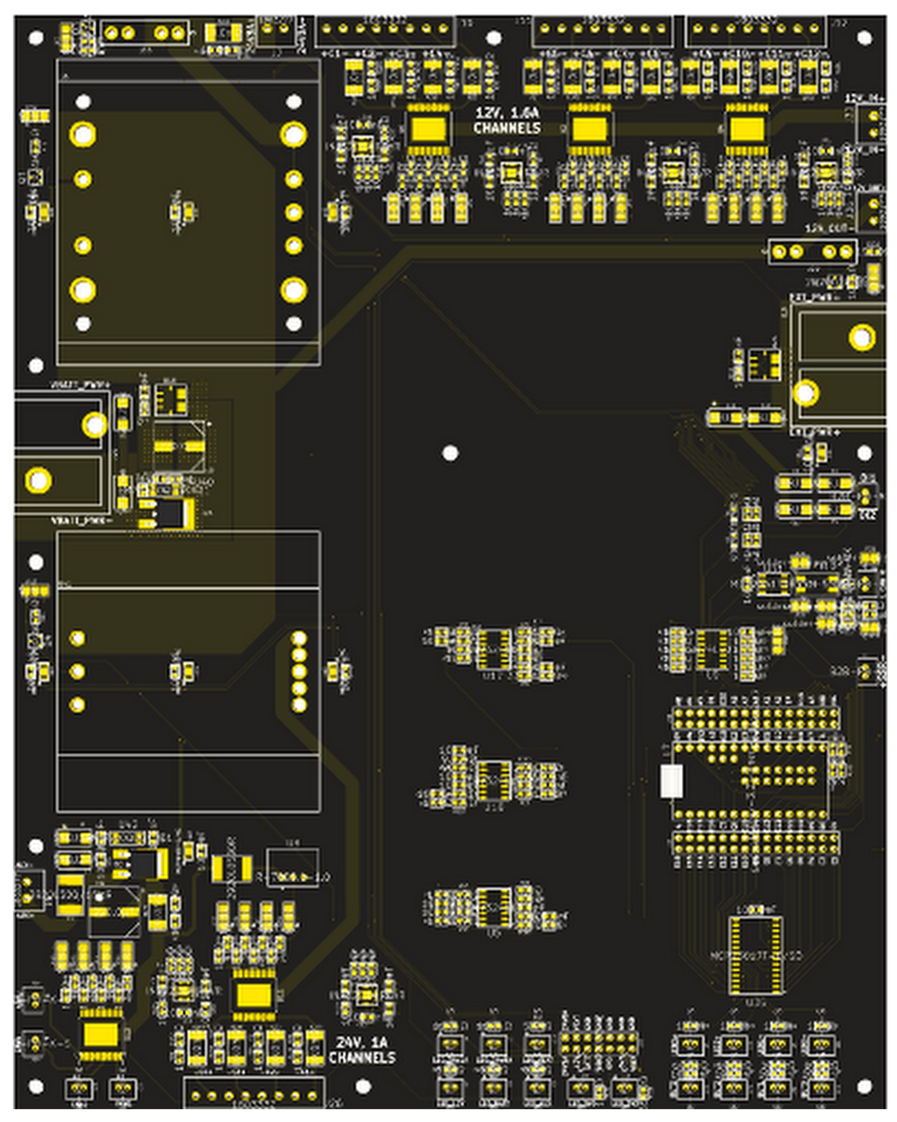
I knew this day would come. Was actually drafting up some requirements for a piece of software with exactly the same functionality – give it a couple ICs and a board outline, get a PCBA out. I would be really surprised if the analog PCB shown above was *really* routed fully by JITx, though.