Electron microscopes were once the turf of research laboratories that could foot the hefty bill of procuring and maintaining such equipment. But old models have been finding their way into the hands of eager individuals who are giving us an inside look at the rare equipment. Before you start scouring Craigslist, go on a crash course of what you need to know with Adam McComb’s Hacker’s Guide to Electron Microscopy. He presented the talk at the 2018 Hackaday Superconference and the recording was just published, you’ll find it below.
Two Ways to Make the Really Small, Big
The first thing you need to know about these instruments is that there are two categories: Transmission Electron Microscopes (TEM) and Scanning Electron Microscopes (SEM).
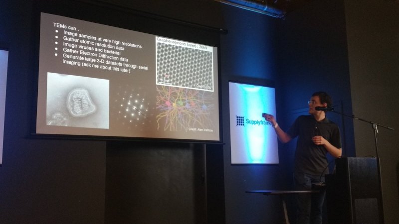
Though it might seem tempting, you probably don’t want to get involved with a TEM. These microscopes operate by shining electrons through a sample onto a phosphor target; the phosphors glow, building the image. With a TEM you can achieve incredible resolution — on the atomic scale — and do things like taking pictures of viruses and even reconstructing neural connections in the brain. But all this comes at the cost of higher complexity. Samples need to be very thin, on the order of 70-100 nanometers, which means you would need access to specialized cutting tools such as diamond knives and ion beam milling. The optical path is incredibly complex, and chemicals to prepare samples can be quite hazardous.
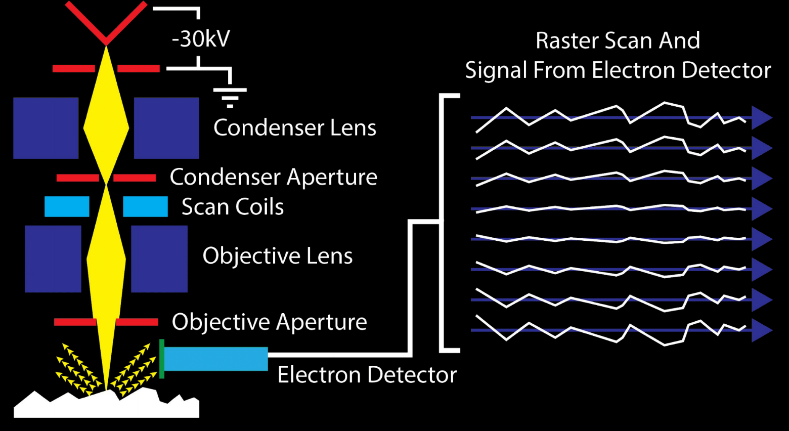
On the other hand, Scanning Electron Microscopes (SEM) are well within reach of the home workshop. They function by aiming an electron probe at a sample and counting the number of electrons that bounce back at each discrete location to judge brightness. These are the instruments that hackers are starting to have in their garages and workshops.
SEM Capabilities and Workflow
In his talk, Adam illustrates some of the extended features of an SEM in examining integrated circuits — you can use one to do much more than simply making pictures. The primary electron beam generates those secondary electrons bouncing back to the sensor to form an image of the surface of the sample. But at higher voltages, backscatter electrons will also be generated which can be used to derive its chemical makeup. With the proper sensing equipment, characteristic X-Rays generated when an excited ion in the sample falls back to its ground state can be used to determine the sample material. Combining these means looking beneath the surface of the die to judge what materials are present and where they go. Effectively you are now reverse engineering the layers in an IC design.
Adam dips into details of the sample prep process, which is much easier than with a TEM but which still requires a bit of effort. Samples need to be electrically conductive so that electrons bounce off instead of being absorbed, and this usually involves sputter in an argon and gold process. Since they will be observed in a vacuum, samples must have very low moisture content, and there are some hacks around that which he shares with us.
Have you played around with SEMs? Share your stories below. We know Ben Krasnow has, since he put an LP record in the SEM. Sam Zeloof has one in his home lab. And there are SEM projects on Hackaday.io such as the efforts Jerry Biehler has been putting into a 1980s-era Hitachi. It feels like a crazy hobby, but neither the knowledge nor the equipment are out of your reach!


I think for DIY the easiest would be to build an Atomic force microscope which was featured here: https://hackaday.com/2014/04/29/a-diy-atomic-force-microscope/ 5 years ago
There is the banana equivalent for radiation. Banana shown for scale.
I got to play with one of these at Nuclear Electric in the UK when I was around 14 on a work experience jaunt. I was amazed when we put a bit of hair in there that it actually looked like the representations shown on adverts for shampoo!
Well, I’m a bit of a fraud in this context, since I’m a professional electron microscopist, but one of the cool things you can do in an SEM is photogrammetry. You take 18-20 images at high tilt angle, rotating the samples around 20 degrees each image, with a couple of images of the top of the sample for good luck, and then run the resulting images through photogrammetry reconstruction software (I like Zephyr’s 3Dflow right now, since it’s free) and you should be able to output a highly magnified 3D model suitable for 3D printing. See some of my examples on my Sketchfab account. We’re on Instagram as well @nhm_imaging
Okay this is a perfect example of someone doing a very specific and Technical job and easily relating something cool about it and usable to an average hacker
Why is this site so ugly now?! Does anyone know when it’ll be fixed?
I haven’t seen it on a computer in maybe a year.
Finally I can read the thing properly on my smartphone which is been my main computer for the last 3 years or so. This site was always really hard to see the text at the far left and in general poorly laid out as a mobile version.
I actually kind of like the new version though I feel they could scale the text down just a hair in size
I have one as well: https://debugmo.de/2018/11/my-scanning-electron-microscope/
It’s an old Zeiss DSM-950, but we’ve added digital image readout (based on a hacked OpenVizsla FPGA board).
I successfully imaged a couple MEMS devices (https://twitter.com/tmbinc/status/1045683618780258305 etc.), DVDs and other optical media (https://twitter.com/tmbinc/status/992020274794115073 etc.) and random other stuff (https://twitter.com/tmbinc/status/1097893078105554945) with it.
Resolution isn’t awesome (yet?), but much better than an optical microscope – roughly 50nm, though it’s spec’ed at 10nm.
It’s a fun toy.
Oh- I thought it was reduced permissions I imposed on my phone for additional illusion of security. It’s sorta’ love-hate, but faster.
Diamond knives and ion beam milling? I’m deeply interested in learning more. Familiar with ulteasonic coring samplers for microscopy, but not these things. Anyone refer to further info?
I don’t know much about diamond knives, but I know quite much about ion beam milling. There are special machines which instead of electron probe/ beam column are equipped with ion probe/ beam column. It s called focused ion beam (or simply FIB). Most common FIB uses some liquid with Ga where it gets extracted at source and is accelerated through collumn (Galium is accelerated as a positive ion, and thus the ion optics in that case would have reverse polarity to that of electron optics). It can be accelerated up to 30kV (this is what I normaly use for milling). The strength of the ion beam (measured in nA – same as electron beam) is regulated by inserting diferent size apertures in the ion path. FIB is normally accompanied with GIS (gas injection system). That casually contain 5 substances which can be applied to the micro-area where we are working with FIB by nozzle inserted very close to the area. There are substances like platinium organic compound, which can be used to coat defined shape (remember we have the focused beam with rastering capability) to increase conductivity. There can be some very agressive substances which gets activated with ion beam and do very efficient etching (XeF – very lethal substance even in very small amounts, but that goez very nicely through some type of hard minerals – and I am geologist). So with right GIS the FIB can be used not only to mill, but also to build up things. The other lab I know has different substances in they GIS, they are specialising in micro-chip prototyping.
So what would interest other here is that with rightly prepared FIB machine one can preciselly in nano scale cut some traces and make other traces and insert/ build up tranzistors into the microchips. It is like 3d printer and cutter in the single tool and for micro/nano scale.
Oh I think I had detoured away from the question.
So FIB nowadays come together with electron column and those are called dual-beam machines (normally electron column is vertically, and FIB on side at 50-60 degrees to electron column). The problem with FIB is that it is very bad at imaging as you are litterally eating the surface away with ion rastering. I don’t say it is impossible – it is possible with the Seconday electron detector, but you will see only the morphology. So with dual beam machine we can have back scatter electron imaging thanks to electron column (and detector of BSE) – so after aligning those beams, we can navigate very preciselly with FIB and cut out exact places we see with electron imaging. We can also observe in real time how milling is going.
Milling.
this is process of displacing atoms by bombardment of highly accelerated Ga ions – the depth is dependant from beam current, milling time and hardness of the milled material. As FIB have rastering capabilty you can mill any shape.
TEM foil preparation.
you chose the place in your sample which you want to investigate. This technique allows to cut out foil perpendicular to the observed surface. After rotating/ aligning the sample so that future foil would be oriented horizontaly two trapezoids are milled away from top and buttom of the future foil. It starts with high current (which is fast but not precise) and the thin structure (future foil) looks like a bridge, so milling away sides of that bridge until we get 1 micron. Then starts the fun, we are milling sides of the bridge with lower currents and that takes longer. Also it is good moment to cut the bridge from both ends, the foil will be holding to the sample by bridge buttom. As we get close to the wished thickness of the foil (for High voltage TEM (200-300keV) 200nm; for STEM on SEM (30kV) 20nm), we tilt the sample and cut the buttom of the “bridge” leaving only a small trace to keep the foil attached to its original sample. Normally machine is equipped with micro-manipulator. I know how to work with needle-based type. Needle is brought very close to the top of the foil, and with help of the FIB and GIS is soldered to it. then the trace at the buttom of the bridge is cutted out, and slowly the foil is taken out from its original position, now supported only by solder with the needle. Futher it is transported to the copper mesh or soldered to the micro-copper finger holders for TEM. The solder with needle then is cutted of.
Highly experienced operator can prepare in this way 1 foil in 5 hourz. The difficulty and possibility to fuck-up that is increasing with every step. For material sciences, where material is known and experimented with prior cutting the thin foil, whole process up to lifting foil-out can be automated. But for geological sample – forget that, every sample is different, and it is common that only 3rd or 4th trial isfinalized with success.
I want to add here one more technique available for dual-beam machines which could be interesting for the readers. The FIB micro-tomography. By cutting/milling away slice by slice and taking electron images between slices we can reconstruct exact 3d model of the composition (do not mix with 3d model of the surface). I see this would be useful at RE currently produced 3d chips.
Last time you did an article like this, an eBay Spectronic 20 showed up courtesy FedEx
I’m in the process of buying a isi-sr-50 with my hackerspace Bitlair, the Netherlands.
Where does a hack like me find information on these devices?
Is there a SEM enthusiast forum with a secret site for manuals from the 80’s?
Thanks in advance.
Anyone knowledgeable or just interested send me a message.
Try to ask someone from https://www.isibrno.cz/
And I thought I was one of the cool kids because I had a Mantis 3D microscope at work…