
From the heart of Silicon Valley comes a new buzzword. Gallium nitride is the future of power technology. Tech blogs are touting gallium nitride as the silicon of the future, and you are savvy enough to get in on the ground floor. Knowing how important gallium nitride is makes you a smarter, better consumer. You are at the forefront of your peer group because you know of an up and coming technology, and this one goes by the name of gallium nitride.
OK, gallium nitride is more than just a buzzword. It is, indeed, important materials science. Gallium nitride is a semiconductor that allows for smaller electronics, more powerful electric cars, better solar cells, and is the foundation of all LED lighting solutions today. Time will tell, but it may well mark a revolution in semiconductors. Here’s what you need to know about it now.
The Early History of Gallium Nitride
You’ve probably got gallium nitride right now in LEDs all around you. Because of the nature of gallium nitride and its wide bandgap, it is idea for optoelectronic applications. What does that mean? First, let’s back up a bit.
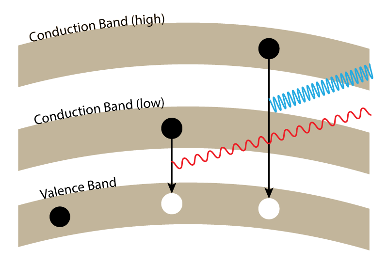 Light Emitting Diodes operation on conduction bands. Put some energy into an atom, and an electron will move into a higher conduction band. The electron will then return to the lower valance band and a photon will be given off. The energy of the photon, and the frequency of this light, is determined by the gap between the valance and conduction band. Move an electron from a valance band to a not-much-higher conduction band, and it will give off infrared or red light when it comes back down. Returning from a further conduction band will give off blue or violet or ultraviolet light.
Although infrared and red LEDs were in production by the mid-to-late-60s, it took until the end of the 90s for blue LEDs to make it into consumer goods. The development of the blue LED was based entirely on gallium nitride technology. This innovation was the focus of the 2014 Nobel Prize in physics, and today gallium nitride LEDs are saving us tons of energy.
In the two decades since the development of the first gallium nitride blue LEDs produced by the Nichia Company, there has been loads of research on using gallium nitride for applications other than optoelectronics. Whether it’s because gallium nitride is just sitting around in a lab, waiting for bored physicists to experiment, or because companies are looking to find more uses for gallium nitride, there are more applications for this semiconductor than ever.
GaN As A Transistor
Beginning in 2009, gallium nitride has been available outside the lab as a replacement for silicon MOSFETs. Because of the high power handling, low power losses, and size reduction, gallium nitride was first used in devices that dumped a lot of current, electric cars included. As with any technology, it eventually makes it into lower-cost items and now gallium nitride can be found in a fantastically small phone charger from Anker. The size of this charger is only possible thanks to the efficiency and power handling capability of gallium nitride MOSFETs. This is highly advanced technology that’s making inroads in consumer electronics in less than a decade.
If gallium nitride is so good at high-power and high-frequency applications, why isn’t it seen in 50-year-old equipment? That answer comes down to simple economics. Before the 90s, there was little application for gallium nitride, as silicon was easier to produce, and the fabs had already built their production lines around that specific technology. In the late 90s and early 2000s, gallium nitride came into its own with blue and white LEDs, and production has been ramping up ever since. With a new technology, there is always room for improvement and now two decades after the first commercial blue LEDs, gallium nitride production is very good. GaN is a mature technology now, and any mature technology will search out new markets.
Enabling Exploration of Hot Planets
As if it weren’t enough that the properties of GaN make it perfect for high-power and high-speed transistors, there is another benefit: high temperatures. As any PC gaming enthusiast knows, silicon doesn’t like high temperatures, and this is a problem if you want to explore Mercury, Venus, or the interior of the gas giants. In research funded by NASA’s Hot Operating Temperature Technology (HOTTech) program, P-N junctions fabricated out of gallium nitride were found to operate very well at temperatures of 500 °C.
This fact alone means that gallium nitride transistors will allow computation in environments where silicon simply doesn’t work. The only exploration from the surface of Venus lasted only about two hours until the electronics fried themselves. The research into using gallium nitride as an electronic switch provided more than twenty days of data, and in the end the transistor still worked perfectly.
Right now the research is only in the beginning stages, but gallium nitride could be the basis for post-silicon computation, forming the gates in CPUs and memories on the surface of other planets.
The Technology That You Need To Know, Now
Yes, gallium nitride can make smaller, more powerful power supplies, but it may also be the future of electronics. It’s already the foundation of modern LED lighting, and it could very well be the technology that broadcasts video from the surface of Venus. It’s a wonder material, and knowing about it now makes you a smarter, better person.


Why did the maker build with silicon transistors?
He bought so many he felt that he needed to keep using them until they were all GaN!
You’re welcome for that.
Ba-dump-tchhhh… :-)
See, here we pronounce it GAHN and now we know why. We have the 2nd sexiest accents up here near Bahstuhn #MarkyMark
https://bigseventravel.com/2019/05/50-sexiest-accents-usa-ranked/
I’ve been working with GaN devices now for a few years. They are still a challenge to utilize, as in switching MOSFETs, but with the proper gate drivers (see TI’s LM5113 and newer replacements), it is definitely helping. I compare it to SiC early MOSFET growth and maturation period. Having said that, I’m fascinated by how fast these devices are capable of switching….
Even more fascinating if find your design meeting class B limits (House hold) with these devices…
10 years ago everyone told you: “relax your slopes!” Now1kV/10ns is kind of OK (efficiency wise)
73
I totally agree. The gate biasing can be tricking unless you have a proper proper gate driver. For faster than normal switching applications, SiC is an EASY drop in replacement for traditional FET’s where as GaN is not.
My first reaction too: ever heard of copy editors? “Valance”?
Are you saying that your bed ruffles do not give off light? If so, better upgrade.
I watched “The Man Who Shot Liberty _Valance_” once!
B^)
You’ve missed idea, which should probably be ideal, so you call yourself an editor? 😉
Sorry, quite unrelated to the article, I’m just curious how which article gets an original artwork and which doesn’t is decided and by whom? Because the artwork on this one is awesome! I wish every article gets one.
That artist really is great.
He truly is. IMHO, it’s one of the biggest differentiators between this and any other tech. blogs. I mean HaD has excellent writers, but the original artwork is second to none.
Yep, the snake on the left, turkey baster, light bulbs, and mustard bottle all go together to spell grant money!
Someone’s bitter.
Joe Kim is HaD’s resident artist,
I’m not sure…
but I think this particular piece has been used before in a HaD banner.
so sorry that enema isn’t working for you guys, maybe a little fiber in your diet would help.
No, the *peak* smarmyness is usually edited out. But you already knew that because you’re an exceptional consumer of media. Thank you very much for your appreciation.
So you’ve gone back to your bad habit of editing critical posts?
Can anyone knowledgeable chime in on how this compares to silicon carbide chips? I know they can operate at temperatures that are horrifyingly hot compared to pure silicon, but it’s outside my expertise far enough I can’t compare them.
I don’t directly have experience in SiC, but from the research papers I’ve read GaN can switch much faster (in the MHz range) while SiC caps out in KHz so magnetics can be much smaller in GaN systems of comparable power.
The last time I discussed GaN vs. SiC, I almost ended up in a fistfight in a bar, so I’ll try to back up my numbers with sources. Let’s compare two roughly equivalent devices that are available today. I selected two devices with a similar Vds/Rdson(150C) ratio, the GS66504B-E01-MR (260 mohm Rdson at Tj = 150 C, 650 V Vds) and C3M0280090J (385 mohm Rdson at Tj = 150 C, 900 V Vds). As the power handling capabilities of both devices are similar, the main parameters of interest are switching loss, gate charge and cost.
Sadly, turn-off loss is not given for the GaN device, so we can only compare the stored output charge. This is surprisingly enough lower for the SiC device (3.5 microjoules at 500 V, vs. 5 for the GaN device).
The gate charge of the SiC device is roughly three times that of the GaN device. Coupled with the lower gate voltage, the GaN device requires significantly less drive power at high frequencies. To put some numbers to this, it would take 180 mW to drive the SiC gate at 1 MHz, but only 18 mW for the GaN device.
When it comes to cost, the SiC device has a clear benefit, at 3.19 EUR in single quantity from Mouser, compared to 12.21 EUR for the GaN device. Pricing for either device does not fall drastically with quantity from the common distributors.
GaN allows you to switch really fast, but it also requires low-inductance packaging and board design to realize this benefit. The power density of magnetics beyond a megahertz or two does not increase significantly, as we can’t make fine enough litz to overcome eddy current (mainly proximity effect) losses at these frequencies. With resonant topologies, you can already get to the point of diminishing returns with SiC devices.
SiC devices are excellent for handling a lot of power at moderate frequencies. I did the hardware design for a 300 kW buck converter with SiC MOSFETs, and we realized over 99 % efficiency at 75 kHz and a 2:1 voltage stepdown ratio, using roughly 300 square millimeters of MOSFET and a similar area worth of SiC schottky diodes.
But there’s no real clear answer. In some applications, the merits of GaN makes it a clear winner, while SiC is the obvious answer for other applications. And in many cases, superjunction silicon MOSFETs and even IGBTs will be the cheapest overall solution. As far as power electronics goes, we live in very interesting times.
To the cost point: GaN will be cheaper in the longrun, SiC technology is just more mature at the moment
The last time I checked, Gallium was rather expensive (on the order of the price of Gold). Of course, there’s not very much Ga in a GaN device. Silicon Carbide is dirt cheap, though.
I would like to drink at the bar where patrons are passionate enough about semiconductors to nearly come to fisticuffs
Once in a bar, I had a high school science teacher tell me that TWT’s were only a foot long,
this was when I worked at a facility that had TWT’s that were a foot wide (and thirteen feet long).
B^)
A mutual friend introduced us because she knew we were electronics nerds, and therefore would probably get along great…
I wish I could thumbs up your comment. Yep, in the end nothing is always better in every scenario, and having multiple options allows flexibility in approaching design for different applications. Also lol, I would love to be a patron of an engineering bar where fights over semiconductors and technical trivia are commonplace! Just gotta be careful of drinking and deriving!
LOL!
The thought of a bar fight breaking out over an argument about SiC vs GaN brings a simile to my face.
Seymour Cray talks about Gallium Arsenide in 1988:
https://www.youtube.com/watch?v=xW7j2ipE2Ck
That’s different, I presume.
Probably nastier to work with due to the arsenic.
We have a very small scale semiconductor fab at the University of Florida that is capable of working with gallium arsenide. The salient features of the building housing it are several large red lights and lots of boxes full of self-contained breathing apparatus located around the exterior of the building. Scary stuff indeed.
Working with as in making chips? Because while GaAs is nasty to make using it isn’t a problem (in normal scenarios) but chip manufacturing in general use very nasty chemicals.
Yep, any chip fab is nasty, GaA, GaN or just plain silicon… lots of potent acids, HCF and such… The arsenic is definitely bad but I’m not sure that’s the worst offender in the fab…
Why GaN? https://epc-co.com/epc/GalliumNitride/whygan.aspx
Ok I get Brian’s (not Brain) writing style can require a let’s just say acquired taste that not everyone will enjoy, but I literally can’t think of how anything in this article could be considered smarmy. It’s a pretty straightforward affair detailing the past, present and future of GaN. As someone who has performed research in grad school right as our lab was getting into GaN, I thought most of what was written was accurate and well laid out. It’s a good article for people who have never heard of the topic, but would appreciate learning more.
One thing that is never mentioned when you hear about all the advantages of GaN, is that to grow large pure crystals is not easy.
Melt grown pure GaN crystals, which is never done, would requires temperatures greater than 1600°C (2912°F) and pressures greater than 45,000 atmosphere (660,000 PSI). Slower, less efficient, but more practical processes are used instead.
GaN devices can operate fine at 500°C but if the cooling system fails and they hit 800°C then GaN dissociates into gallium metal and nitrogen gas, and the device is kaput.
Production challenges is one of the reasons that Si devices are still so common – it’s just SO much easier to manufacture than most of the competition, including the extreme ease of growing gate material (just oxidize your substrate).
GaN has lots of advantages, but it’s a PITA to manufacture devices with it. This WAS mentioned in the article by reference to the fact that Nakamura figuring out how to manufacture devices with it merited a Nobel Prize for him and his associates.
A reference to the Nobel prize for blue LED’s is an extremely indirect way of saying that the Czochralski process can’t be used to grow large GaN wafers. But maybe you saw something that I missed, I did click and read all the links that I could.
What I’m wondering is… are there any common chip packaging and circuit assembly technologies that can operate at 500C, if we wanted to put these things into a Venus lander? FR-4 PCBs would start to decompose and lead-tin solder would melt at those temperatures.
Ceramic packages are a thing for space and military-grade electronics. As for lead connections, ultrasonic welding would negate the need for solder. I say this from vague knowledge, but surely someone here knows more about the techniques used in the original Venus landers….?
Exactly that. Welded connections like in the Apollo Guidance Computer. Ceramic circuit boards are a thing, although I don’t know if the commercially available ones can withstand 500C. One manufacturer says theirs are good to 350C.
There are probably exotic ceramic materials that can go higher. Shuttle tile? Or Aerogel, maybe?
If you can design and package chip that work at 500°C, the welding to ceramic substrat is probably not a major issue…
“The development of the blue LED was based entirely on gallium nitride technology.”
The first commercial blue leds were based on Silicon Carbide which was dumped when they figured out how to make GaN blue leds.
Though the first blue GaN led actually happened in 1972
https://spectrum.ieee.org/tech-talk/tech-history/silicon-revolution/rcas-forgotten-work-on-the-blue-led
I was about to say the same thing. I had a handful of Silicon Carbide blue LEDs back in about 1985, but the efficiency was awful, and the color was rather sickeningly pale.
So would this be useful for cpu chips or is it not right fir that application? The difficulty growing large crystals mentioned upthread would probably be an obstacle.
> would this be useful for cpu chips ?
For GaN, I’d say yes and no at the exact same time. No for implementing current designs and yes for possible future designs.
The thing that slows down conventional CPU’s is that it take a lot of energy and time to turn transistors on (and off), the circuits take time to charge up, and discharge. The smaller you make the circuits the faster you could switch them, because less electrons are required to change states, but then you hit the second problem which has limited the clock rate to in and around around 2 to 4GHz since about 2003, as you increase the circuit density you have more thermal energy per unit area that you need to dissipate to stop the chip from literally evaporating. So cooling technology has been limiting the clock rate, it is not easy to cool a tiny area that could reach insane temperatures ( ref https://slideplayer.com/slide/12890952/78/images/13/Power+Is+Another+Big+Problem%21%21.jpg ). In fact to avoid insane cooling systems clock rates have been going down as the process has gotten smaller, but core counts have been increasing.
So where does GaN fit into this picture, instead of using electrons to change states, GaN could generate photons, which would generate less heat, and also have a faster switching time. But if you are using photons, then there is also the potential to use the quantum state of the photons…..so that could be interesting future path as well.
“> would this be useful for cpu chips ?
For GaN, I’d say yes and no at the exact same time.”
If you say “yes” and “not” at the exact same time,
does it come out “nyet”?
B^)
yesn’t ;)
Interconnect propagation delay is becoming more dominant. As you go for higher density, you also shrinks the cross-sectional area of the tracks which means higher resistance. Larger R means more R*C delay. One way is to break up long signal tracks into shorter segment and put in buffers between them.
There will be diminishing return going to smaller and smaller geometries even if we were to switch to different types of transistors. The cost for designing (more complexity) and manufacturing (more process steps) smaller geometries seems to go up geometrically.
Interconnects also space out the chiplets over a much larger area so less heat per unit area, with the benefit of slower lower power cooling solutions.
If you reduce the length and width of tracks by the same percentage and keep the height the same then the resistance would actually be lower ( https://en.wikipedia.org/wiki/Electrical_resistivity_and_conductivity )
I fully agree then going smaller and smaller is nearly as small as it can go. It is getting close to the stage where natural background radiation will glitch devices.
As far as I’m aware GaN has a very difficult time being used as CMOS, and you have to design it as a pull up/pull down circuit, so during some states there exists a path from source to ground. So even though normally off GaN HFET are very fast, because normally on transistors aren’t you either have a circuit that consumes a lot of power, and thus creates a lot of heat, or you have to run at the normally off HFET speed, making Si transistors better. This can’t be solved by new manufacturing techniques that would allow you to easily grow large GaN crystals at low temperature. (Let me know if I’m wrong with the CMOS thing, my design sources on this are based off of GaAs)
I remember the first project I put a blue Led into. A amplifier for on hold music at a company. Thought I’d be cool and use a blue Led since they finally were available and less then $10! Late 90’s etched the board for amp and everything, now don’t even remember how to! Should have heard the on hold music that the phone system had from maker, bleh! Hooked amp up to satellite receiver and had whatever music they wanted and could hear it. Also put output for music in office so employees could listen.
No comparison to silicon-based semiconductors in terms of parameters. No mention why its so much better to use. No cost-comparisons. Only Benchhoff-cynism that increasingly sound like he needs a hug. Sorry, but thats not up to hackaday-standards.
Me too noticed this error.
You’re wasting your fingers… People have been complaining about it since I came here over a decade ago..
It is interesting and important technology, but the appeal to being a better consumer is perhaps mistaken.
When the term is used in marketing and packaging, I can guarantee you it will often be a mere keyword. An educated consumer should consider the final specifications of the device, and not get caught up in “OOooh, GaN!” You can absolutely use enough GaN somewhere in a design to write it on the box, and yet, have a low quality device being sold at premium prices. Expect it!
It might even be that the more you believe this improves your knowledge as a consumer, the less it helps.
GaN blockchain is going to be a blockbuster
Just as an example, a big issue robotics applications have like exoskeletons or surgical robots is the heat generated by traditional servo drives or motor controllers using silicon transistors. With GaN, the switching losses are considerably reduced thus enabling this sort of applications. I believe there is only one company that has developed servo drives with GaN, its called Ingenia https://ingeniamc.com and has recently been acquired by a public US company. Looking forward to see the new robotics applications GaN technology will enable!
Do Ingenia make space-grade servo drives? Looks like they are now part of Celera Motion.
Dope. I regularly wish Apple would make a smaller MacBook charger, it seems so off-brand for Apple to have this big awkward brick to charge their slim laptop (although I do appreciate it over some PC laptop adapter bricks for sure).
Can’t wait for the prices to really plummet on these devices — I see great application for these as class E RF output devices. With the low on resistance and low output capacitance some of them have, it’ll make for interesting designs.