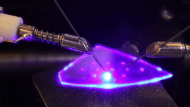
An irregular shard of a crystal wafer is set on a table, with two wire probes contacting it. Between the probes, a bright blue-purple light glows, illuminating the rest of the wafer.

Making LEDs In The Home Fab

Impressive as it most certainly is when an amateur fabricates a semiconductor, most of the projects we’ve seen are more demonstrations than workable chips. [Dr. Semiconductor], however, is going much further with his fabrication process, and is already working on a method to bond chips to printed circuit boards. It’s difficult to align a PCB with the pads on the underside of an opaque silicon wafer, however, so as a trial run he’s made and bonded some transparent LED chips.

The starting material for these chips is a gallium nitride (GaN) LED epiwafer, a stacked structure of n-doped GaN, an indium gallium nitride quantum well layer, and p-doped GaN grown on a sapphire substrate. When current passes through the structure, electrons from the n-doped layer and holes from the p-type layer recombine in the quantum well layer, emitting blue light. To make a functional LED from this, [Dr. Semiconductor] needed to make electrical contacts to both the n-type and p-type layers. Making the n-type contact required cutting through the p-type and quantum well layers.

This would normally be done with reactive ion etching in chlorine, but [Dr. Semiconductor] came up with a new process: a 355-nm ultraviolet etching laser causes GaN to break down into gallium and nitrogen, with the resulting cut being cleaned up by a potassium hydroxide etch. To deposit the contacts themselves, [Dr. Semiconductor] formed a photoresist mask, deposited metal (nickel, silver, and titanium) in a sputtering chamber, and used a developer solution to dissolve the mask and lift off the unwanted metal regions.
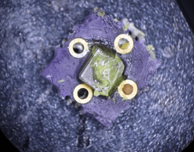
A square, purple PCB is shown under a microscope. The PCB has four vias surrounding a transparent chip, which has a blob of translucent yellow material on top of it.
The LED after bonding and phosphor application.

When [Dr. Semiconductor] applied current between the two contacts, the LED glowed bright blue. The next step was to mount it to a PCB; to do so, he first sliced the wafer into individual LED chips with the ultraviolet laser. He then electroplated indium bumps onto a printed circuit board, positioned the chip above these bumps, added some rosin flux, and melted the indium bumps. This soldered the chip to the board and let the board power the LED.

Like most commercial LEDs, these were blue; most LED assemblies additionally include a phosphor layer which absorbs blue light and emits another color. To create a white LED, for example, [Dr. Semiconductor] mixed cerium-doped yttrium aluminium garnet phosphor power with clear silicone and spread it over the LED. This absorbs some of the blue light and emits yellow light, and the resulting mixture of blue and yellow light looks white to human eyes.

We’ve previously covered some of the history of LEDs and the phosphors which make them useful. This seems to be the first inorganic LED we’ve seen, but we’ve also seen a few homemade OLEDs.

Thanks to [SpuriousIndices] for the tip!

GaN Charger Teardown Reveals Value Of This New Technology

Every so often, a new technology comes along that offers a broad range of benefits over what we already have. Just as lithium-ion batteries have made nickel-cadmium cells boring and old hat, gallium nitride semiconductors are making silicon parts look unimpressive by comparison. [Brian Dipert] looked at what this means in a practical sense by tearing down a GaN phone charger.

The charger in question is a 30 watt USB-C charger produced by Voltme. It cost [Brian] just $10, as prices of GaN hardware have come down significantly as economies of scale have kicked in. The charger measures just 1.2×1.3×1.2 inches, and weighs only 1.5 ounces. That compact size is thanks to GaN semiconductors, which are able to run cooler at higher power levels than their silicon forebearers.

Cracking into the charger required levering open the case. The back panel came off with some work, revealing the mains terminals, which deliver AC power to the PCB inside via the case holding them in contact. Interestingly, the entire circuit inside is filled with an adhesive thermal goop, which helps pass heat from the hottest components to the charger’s case. [Brian] is able to guide us through the circuit, and he identified many of the major components. However, some of the markings on chips were beyond his research skills, and he asks any knowing readers to contribute their own information.

It’s interesting to see just what makes the high-powered compact chargers of today tick. Plus, it’s a hallmark of progress that what was once considered a wonder material can now be had in a $10 commodity phone charger from Amazon. How times change!

The Gallium Nitride Revolution

[Asianometry] has been learning about gallium nitride semiconductors and shares what he knows in an informative video you can see below. This semiconductor material has a much higher bandgap voltage than the more common silicon. This makes it useful for applications that need higher efficiency and less heating.

The original use of the material was for LEDs, but we are seeing increasing use of the material in high-power applications like chargers. Phone chargers are especially common using this technology. This isn’t surprising when your think about how many phone chargers are needed worldwide every day.

Other places that need power-efficient devices are data centers, electric vehicles, and battery-operated equipment. It isn’t clear, though, that we can make enough of the material to meet global demand if it becomes extremely popular. This is especially true because the machinery and processes used to create silicon devices don’t work with gallium nitride. Silicon carbide is a competitor, and it could be easier to create, even though it isn’t as efficient as gallium nitride.

We’ve looked at gallium nitride before, and we are sure we are going to be seeing it again. Silicon carbide may one day operate on the surface of Venus. You can even use it to make homemade LEDs.

Continue reading “The Gallium Nitride Revolution”

DIY USB Charging The Right Way

Since the widespread adoption of USB 1.1 in the 90s, USB has become the de facto standard for connecting most peripherals to our everyday computers. The latest revision of the technology has been USB 4, which pushes the data rate capabilities to 40 Gbit/s. This amount of throughput is mindblowing compared to the USB 1.x speeds which were three to four orders of magnitude slower in comparison. But data speeds haven’t been the only thing changing with the USB specifications. The amount of power handling they can do has increased by orders of magnitude as well, as this DIY USB charger demonstrates by delivering around 200 W to multiple devices at once.

The build comes to us from [tobychui] who not only needed USB rapid charging for his devices while on-the-go but also wanted to build the rapid charger himself and for the charger to come in a small form factor while still using silicon components instead of more modern gallium nitride solutions. The solution he came up with was to use a 24 V DC power supply coupled with two regulator modules meant for solar panel installations to deliver a staggering amount of power to several devices at once. The charger is still relatively small, and cost around $30 US dollars to make.

Part of what makes builds like this possible is the USB Power Delivery (PD) standard, which has enabled all kinds of electronics to switch to USB for their power needs rather than getting their power from dedicated, proprietary, and/or low-quality power bricks or wall warts. In fact, you can even use this technology to do things like charge lithium batteries.

Continue reading “DIY USB Charging The Right Way”

The Amazing New World Of Gallium Nitride

From the heart of Silicon Valley comes a new buzzword. Gallium nitride is the future of power technology. Tech blogs are touting gallium nitride as the silicon of the future, and you are savvy enough to get in on the ground floor. Knowing how important gallium nitride is makes you a smarter, better consumer. You are at the forefront of your peer group because you know of an up and coming technology, and this one goes by the name of gallium nitride.

OK, gallium nitride is more than just a buzzword. It is, indeed, important materials science. Gallium nitride is a semiconductor that allows for smaller electronics, more powerful electric cars, better solar cells, and is the foundation of all LED lighting solutions today. Time will tell, but it may well mark a revolution in semiconductors. Here’s what you need to know about it now.

Continue reading “The Amazing New World Of Gallium Nitride”