
In the hacker and DIY community, there are people who have exceptional knowledge and fantastic tools. These people are able to do what others could only dream about, and that others can only browse eBay looking for that one tool they need to do the job. One of these such people is [John McMaster]. He is the resident expert on looking inside integrated circuits. He drops acid on a chip, and he can tell you exactly how it works on the inside.
At the hardwear.io conference, [John] shared one of his techniques for reverse-engineering intgrated circuits. He’s doing this by simply looking at the transistors, and looking at the light they give off. He’s also looking at the wrong side of the die.
The technique [John] is using is properly called backside analysis, or looking at the infrared emissions of electron recombinations. This happens at the junction of every transistor when it’s active, and these photons are emitted at the bandgap of silicon, or about 1088 nm, far into the infrared. This sort of thing has been done before by [nedos] at CCC in 2013, but rarely have we seen a deep dive into the tools and techniques needed to look at the reverse side of an IC and see the photons coming off.
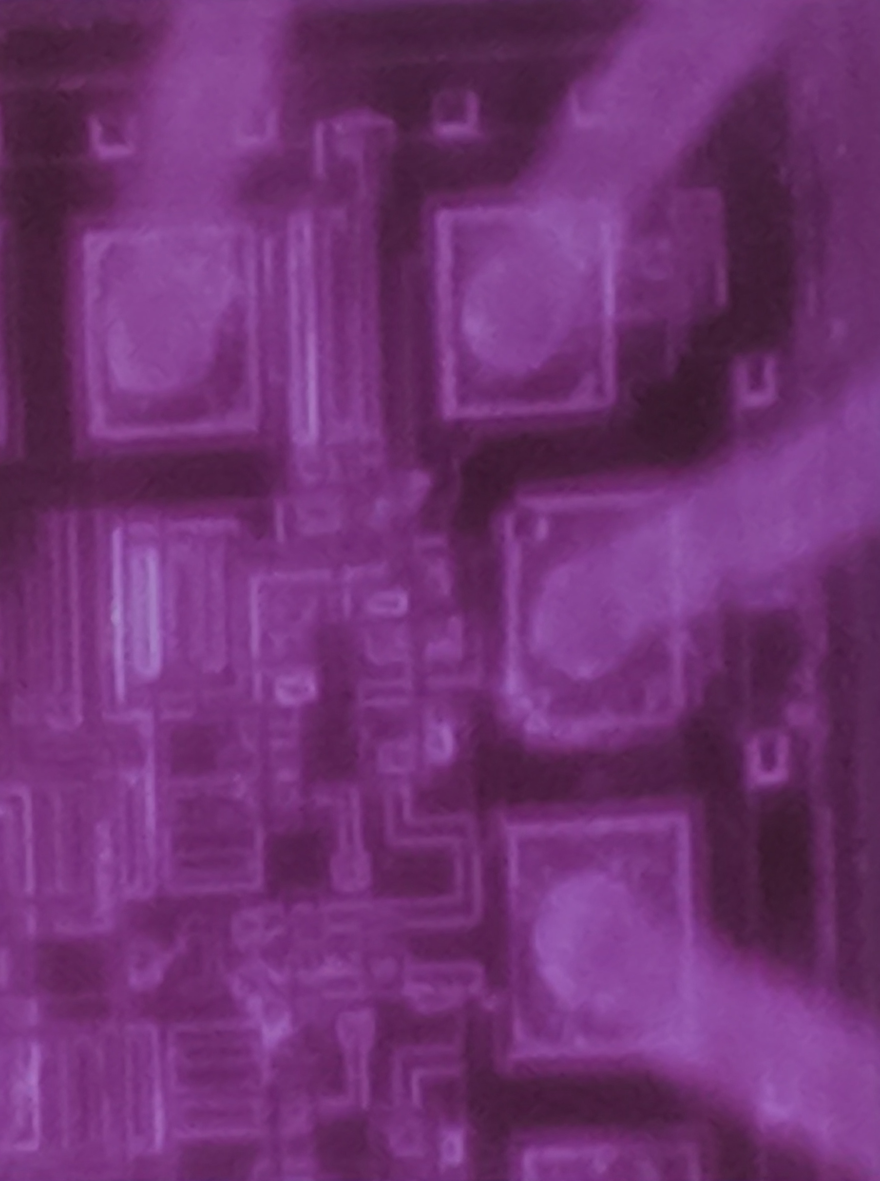
There are several tools [John] used for this work, and he actually did a good comparison of different camera technologies used to image infrared photon emissions from integrated circuits. InGaAs cameras are expensive, but they offer high sensitivity. New back-illuminated CMOS cameras and cooled CCDs normally reserved for astrophotography were also tested, and as always, you get what you pay for; the most expensive cameras worked best, but there were ways you could make the cheap ones work.
As with any camera work, preparing the lighting is of utmost importance. This includes an IR pass filter, and using only LED lighting in the lab with no sunlight, incandescent, or halogen light bulbs in the room — you don’t want any IR, after all. A NIR objective in the microscope was sourced from eBay, for about 1/10th the normal cost, because the objective had a small, insignificant scratch. Using this NIR objective made the image twice as bright as any other method. You can successfully image a chip with this, and [John] tested the setup on a resistor inside a CD4050 chip; the resistor glowed a slight purple, the color you would expect with infrared sensors. But can it work with I/O levels in a more modern chip? Also, yes. It needs some Photoshop to process, and stretching the 12-bit or 16-bit color space into an 8-bit color space, but it does work.
Finally, the supreme achievement of doing backside IR analysis. Is that possible with even this minimal setup? This requires some preparation; the silicon substrate in an IC is transparent in IR, but there is attenuation and this is especially important when the substrate is 300 um thick. This needs to be shaved down to about 25 um thick, which surprisingly is best done with fine sandpaper and a finger.
While few IR emissions were observed via backside emissions, the original plan wasn’t to completely analyze the chip, but merely to do some floor planning. For this, it worked. It’s a remarkable amount of work to see the inside of a silicon chip.


At a wavelength of 1088 nm one could likely not go all that far into smaller manufacturing nodes though.
If I would be optimistic, maybe one could still potentially be able to discern details at about 450-500nm nodes, but smaller I would guess require some other method. (Though, my knowledge on optics in this domain isn’t all too extensive…)
But it would at least give far more information then no information for sure. And together with some later SEM passes, a bit of polishing between each, and some ample amount of time looking over the data, one could likely reverse engineer almost any chip.
After all, even a manufacturing node at sub 20 nm tends to spread out transistors so they look miles apart for thermal reasons (unless its memory, it doesn’t create as much heat), so shouldn’t be too hard to gather some information from it.
Nice article Brian :
FYI : To answer some of the questions in the comments… Many IC manufacturers have expensive equipment to enable silicon level chip failiure analysis. There are a lot of techniques to modify/edit (FIB) , to stimulate and to observe IC operation. From nano probes to lasers , sem, IR, optical and similar to this article photon sensing.. This is a very powerful technique for debugging digital cmos circuits. In simple terms …from the backside of the device I can see any cmos transistor switching, I can generate the timing waveform. It is like having an logic analyzer or oscilloscope probe you can put on any transistor, without loading it down. I have done this myself down to 40nm cmos on an older analysis machine. I have heard public claims of much lower capability. (10nm in link below)
We used to use the multi-probe sem backscatter machines for topside wire switching analysis but not so much anymore.
If designers don’t take measures to protect from this type of analysis….a lot of information can be determined (with enough money and time…). So Alexander I believe your second paragraph comment is correct. As an example, it took me ~2 weeks part time to get all the info to debug inside a crypto accelerator. Half of that was material prep work.
Here is some interesting public info from a manufacturer I found with a DDG hit :-
https://www.fei.com/products/electrical-analysis/
Going down to 10 nm is way more impressive then I expected and would yield a lot more information about what one might be looking at. Though, if I understand the mechanism correctly, it wouldn’t really be helpful at all in tracing out the connections. But that can always be worked out given enough information/time/effort.
Though, what methods could a manufacturer take against this form of analysis?
Putting on a surface coating on the chip wouldn’t do much, since it can be removed.
So only thing left I can think of is to simply make the chip so power hungry that it literally burns up if not covered by a heatsink.
Other than making an overly convoluted design with 3D stacked transistors to simply make people confused and give up, but that gets very expensive very quickly in production and likely won’t keep competitors away from reverse engineering it regardless, especially if the chip happens to be good at what it does…
Alexander,
yes for the connections or localization of area of interest.. You can use several techniques, basic layer-stripping, mosaic assembly and optical image enhancement to create a navigation database for these tools. or use specific code written to activate the area of interest and use one of the sem/lcd/ir or other techniques to quickly narrow down the area of interest. Structures like sram/rom/ are much easier to figure out than random logic from looking at them with just a decent optical microscope. So their in/out ports are examples of obvious points of interest. Even if the buses are scrambled, goto the sense amps.. If it is encrypted at rest if you dump the contents then you have a chance to brute force it in the cloud. Of course reading in the GDSII is easier if you have it available (which is the case when debugging your own chips).
Anyway once the area of interest is localized , you can see through the silicon somewhat so can follow very local connections in the lower metal layers (they are closest to the backside surface) . The deeper connections are harder to follow without reverting to other techniques.
I can’t talk much about your second question .. :)
If a chip contains information that is highly valuable, time , lots of money, equipment, expertise, tenacity, patience all help.. The sheer complexity of advanced chips does make the manual techniques harder so the ROI would have to be there. This is one reason no one should use the same master key for all devices.
Interesting idea. I thought about this and figured it should only work on bipolar transistors. Hopefully there will be a video.
1088 nm is NEAR infrared. That’s all.
I remember reading about using liquid crystal to detect voltages on a chip. Similar to a LCD, voltages would change the polarization of the liquid crystal which can be seen with polarizers.
I also watch a documentary where they use specially synthesized electroluminescence proteins to “see” electrical activities of neurons for mapping out regions of the brain.
When I was at Data General, we had a failure analysis lab. The guys there did a demo with their electron microscope and a decapped chip. You could see the states of the various metal layer conductors, because the voltage level was different and the current flow varied according to the logic level, creating different shades of grey for ones and zeros. Then, they slowly clocked the chip, and the patterns changed.
Very cool. That would have been fascinating to view.
Well, fear no more on missing out: https://www.youtube.com/watch?v=eoRVEw5gL8c
Seeing that would’ve been awesome
Wow amazing. It is unfortunate that here in the UK the term “backside analysis” would suggest a procedure that has nothing to do with silicon!
Seems like this could be very useful for dumping things like masked ROMs that cannot be visibly decoded.
Masked ROMs can be easily decoded if you remove the upper layer of metal or two…
This is so cool! Awesome…
This is so freakin’ cool.
IBM had a research project in the mid-90s which seeked to visualise the operation of a complex chip in a very similar way. It is called PICA, or Picosecond Imaging Circuit Analysis, and was very extensively used by IBM to help debug large VLSI chips during design testing.
Here is a talk by John McMaster from hardwear.io USA 2019 on Low-Cost IC Emission Reverse Engineering/Infrared Light for Reverse Engineering –>
https://media.hardwear.io/low-cost-ic-emission-reverse-engineering-john-mcmaster/