If you’re a space fan, these are very exciting days. There’s so much happening overhead that sometimes it can be difficult to keep up with the latest news. Artemis I just got back from the Moon, the International Space Station crew are dealing with a busted Soyuz, SpaceX is making incredible progress with their Starship architecture, CubeSats are being flung all over the solar system, and it seems like every month a new company is unveiling their own commercially-developed launch vehicle.
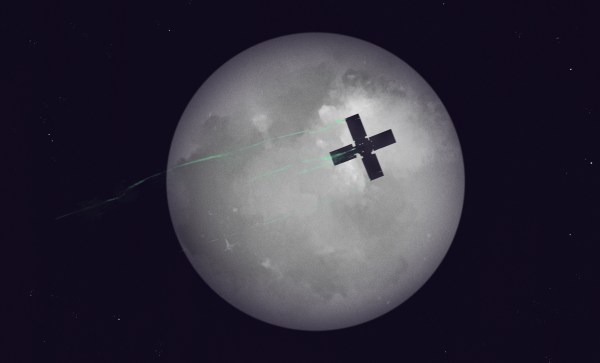
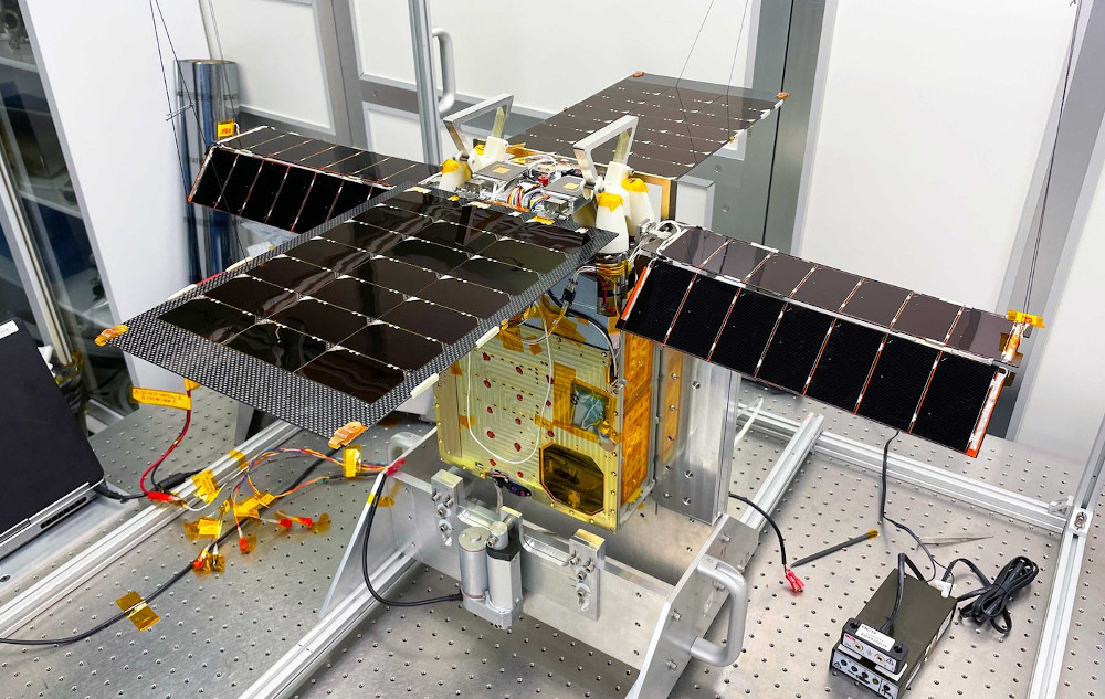
Lunar Flashlight
So with everything going on, we wouldn’t be surprised if you haven’t heard about NASA’s Lunar Flashlight mission. The briefcase-sized spacecraft was launched aboard a special “rideshare” flight of SpaceX’s Falcon 9 rocket back on December 11th — tagging along with two other craft heading to our nearest celestial neighbor, the Japanese Hakuto-R lander, and a small rover developed by the United Arab Emirates. There was a time when a launch like that would have been big news, but being that it was only the second of seven launches that SpaceX performed in December alone, it didn’t make many headlines.
But recently, that’s started to change. There’s a growing buzz around Lunar Flashlight, though unfortunately, not for the reasons we’d usually hope. It seems the diminutive explorer has run into some trouble with its cutting-edge “green” propellant system, and unless the issue can be resolved soon, the promising mission could come to an end before it even had a chance to start.
In the hacker and DIY community, there are people who have exceptional knowledge and fantastic tools. These people are able to do what others could only dream about, and that others can only browse eBay looking for that one tool they need to do the job. One of these such people is [John McMaster]. He is the resident expert on looking inside integrated circuits. He drops acid on a chip, and he can tell you exactly how it works on the inside.
At the hardwear.io conference, [John] shared one of his techniques for reverse-engineering intgrated circuits. He’s doing this by simply looking at the transistors, and looking at the light they give off. He’s also looking at the wrong side of the die.
The technique [John] is using is properly called backside analysis, or looking at the infrared emissions of electron recombinations. This happens at the junction of every transistor when it’s active, and these photons are emitted at the bandgap of silicon, or about 1088 nm, far into the infrared. This sort of thing has been done before by [nedos] at CCC in 2013, but rarely have we seen a deep dive into the tools and techniques needed to look at the reverse side of an IC and see the photons coming off.
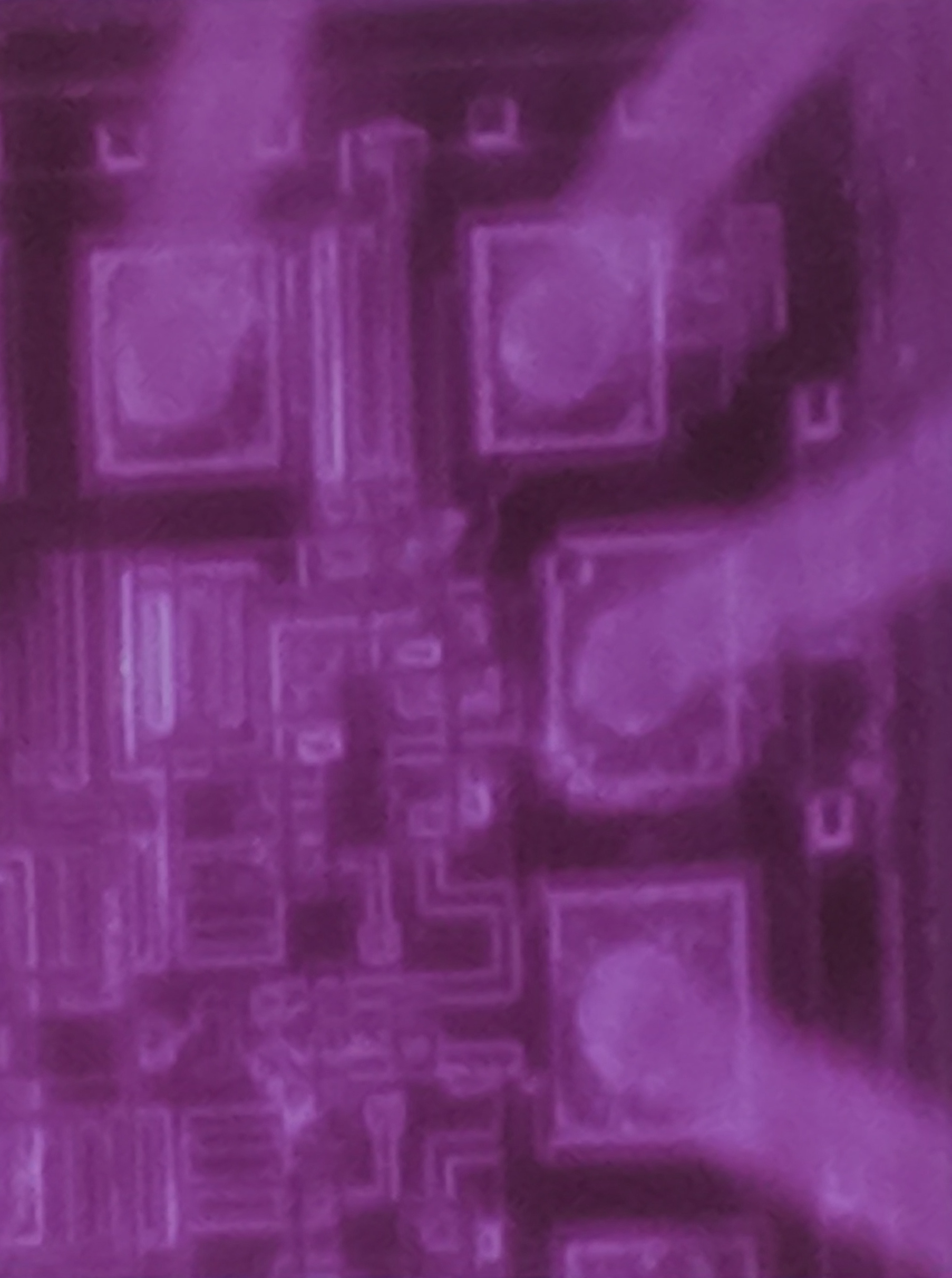
An IC, seen in infrared
There are several tools [John] used for this work, and he actually did a good comparison of different camera technologies used to image infrared photon emissions from integrated circuits. InGaAs cameras are expensive, but they offer high sensitivity. New back-illuminated CMOS cameras and cooled CCDs normally reserved for astrophotography were also tested, and as always, you get what you pay for; the most expensive cameras worked best, but there were ways you could make the cheap ones work.
As with any camera work, preparing the lighting is of utmost importance. This includes an IR pass filter, and using only LED lighting in the lab with no sunlight, incandescent, or halogen light bulbs in the room — you don’t want any IR, after all. A NIR objective in the microscope was sourced from eBay, for about 1/10th the normal cost, because the objective had a small, insignificant scratch. Using this NIR objective made the image twice as bright as any other method. You can successfully image a chip with this, and [John] tested the setup on a resistor inside a CD4050 chip; the resistor glowed a slight purple, the color you would expect with infrared sensors. But can it work with I/O levels in a more modern chip? Also, yes. It needs some Photoshop to process, and stretching the 12-bit or 16-bit color space into an 8-bit color space, but it does work.
Finally, the supreme achievement of doing backside IR analysis. Is that possible with even this minimal setup? This requires some preparation; the silicon substrate in an IC is transparent in IR, but there is attenuation and this is especially important when the substrate is 300 um thick. This needs to be shaved down to about 25 um thick, which surprisingly is best done with fine sandpaper and a finger.
While few IR emissions were observed via backside emissions, the original plan wasn’t to completely analyze the chip, but merely to do some floor planning. For this, it worked. It’s a remarkable amount of work to see the inside of a silicon chip.