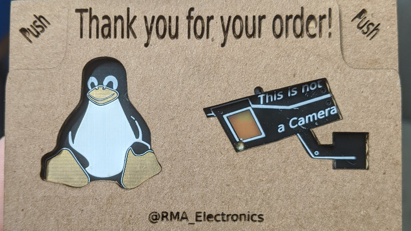
A laser cutter is a useful tool to have in any workshop. While many hackers use them for their cutting abilities, it’s important to remember that they can be great as engravers, too. [Wrickert] was well aware of this when he set his to work, producing attractive packaging for his Tindie orders.
[Wrickert] sells a variety of small PCB-based devices on Tindie, and it’s nice to have something to package them up with, rather than just sending a bare board. To do this quickly and effectively, KiCAD is used to help generate the packaging from the original PCB geometry itself. The board outlines are exported as an SVG file, reopened in KiCAD, and then used to create the required cardboard parts. The laser can then also be used to engrave the cardboard too.
It’s a tidy packaging solution that requires no messy inks or printers, and can be designed in the same software as the device itself. We’ve covered this area before, talking about what it takes to go from a home project to a saleable kit. If you’re in the game, you might find [Wrickert]’s hack to be just the ticket!


I have occasionally cut packaging for things with my 40W CO2. More like cardboard mailers for a bunch of microsd cards or a snug-fit for a pcb so it isn’t swimming around inside an envelope.
However, along parallel lines, exporting the outline layer, along with mounting screw holes has been handy for etching specific positions for drilling holes or epoxying standoffs for mounting some of my projects. acrylic faceplates with openings spaced and sized just right for indicators or buttons for instance.