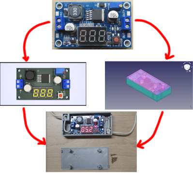
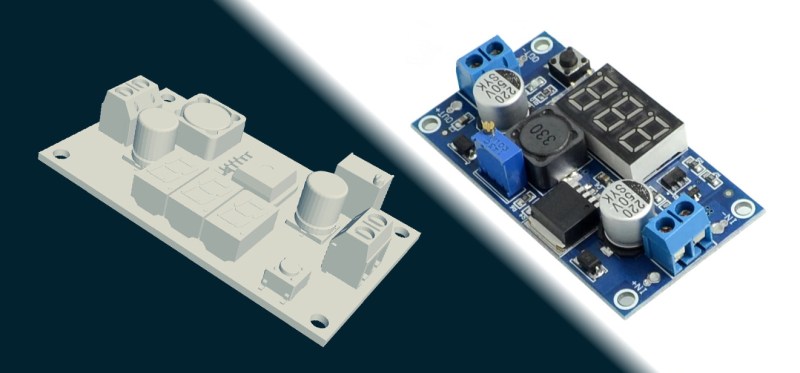
If you’ve used KiCad before, you’re certainly familiar with the handy 3D view that shows you a rendered view of what your assembled board would look like. But as [Vadim Panov] explains, you can take this capability a step further. With a few extra tools and a little bit of know-how, you can leverage KiCad’s PCB renderings to make custom 3D printable enclosures.
The first step is to design the PCB as you normally would in KiCad. This could be an original PCB of your own invention, or a digital representation of an off-the-shelf model you want to build an enclosure for. If the latter, then the PCB doesn’t need to be 100% accurate; the goal is really just to get the big components into roughly the right areas so you can get the clearances right. Though obviously you’ll want to make sure the board’s outer dimensions and mounting hole locations are recreated as accurately as possible.
 From there, [Vadim] recommends a tool called StepUp. This will take your PCB KiCad PCB files and create either a STEP or STL file of the assembled board which can be imported into your CAD package of choice. For the purposes of this demonstration he’s sticking with FreeCAD, as he likes the idea of it being a completely FOSS toolchain from start to finish.
Now that you have a model of the PCB in your CAD software, the rest is up to you. Naturally, there are existing enclosure models you can use such as the ones produced by the “Ultimate Box Maker” that we covered previously, but you could just as easily start building a new enclosure around the digital PCB.
Looking for a bit more guidance? As it so happens, our very own [Anool Mahidharia] will be presenting a class on how you can develop a KiCad + FreeCAD workflow as part of our recently launched HackadayU initiative.


I used to extrude the footprint shapes to what I measure and use that as a reference. For existing ready made PCBs I like to use a 2D scanner to get a fairly accurate placement. It’s better than photographing as that will introduce lens and perspective distortions.
But it’s great that free software now has the option to produce 3D representations of the design!
KiCad already has a tool to export STEP and wrl files of your board. You can import both files into, other modelling software, like FreeCad (That is how I do my Projects). You could do that also with a kicad extension before, in Kicad 4, but it was a bit buggy.
Now you just go to the File Tab in Pcbnew, click on export and click on vrml (for wrl file) or on STEP fro STEP Files.
As long as your components are correctly placed in the 3d viewer (And if they are not, you can place them by hand correctly), you will get a good model of your pcb
Oh. That’s where that is! Thanks! I wasted a lot of time looking for that.
I kept pressing Alt-3 to open the 3d viewer. It has options to export to 2d bitmaps and the edit menu even has an option “copy 3d image” which I think copies the model to the clipboard. I haven’t figured out what program can then accept the model pasted into it though.
I wonder why they don’t have export to step/vrml options in the 3d viewer. Wouldn’t that make a lot of sense?
I guess because the 3d viewer is just a viewer. Not the renderer. I would say the renderer is inside of Pcbnew. A hint that this is so, is because allways when you make a change inside of Pcbnew in the pcb, you can see instantly the changes in the 3d viewer, without making a reload (Or hitting a button to reload the model)
But yeah, you are right, they could also put the export button in the 3d viewer.
But it also makes sense to put all the exports (spectra, step and wrl) inside a single tab, where the model is designed
Actually that would made a lot of sense, they have all fab outputs in one place but this would be nice alternative location that is intuitive…
Yes, but with the StepUP tool, you can do a lot more than KiCAD’s exporter. StepUP is designed to “marry” KiCAD and FreeCAD. You can easily push-pull between the two packages. StepUP can also be of great help in aligning the 3D models with the footprints. With StepUP you can also export the traces, vias (even blind and buried), which is of great help when you want to do 3D electromagnetics simulations. The beauty of StepUP is that you can adjust the position of components in FreeCAD, e.g. to avoid mechanical collisions, and then push those changes back to KiCAD. I have not gone back from the 3D electromagnetics simulator to KiCAD yet, though, but this is a serious problem with commercial packages as well, e.g. optimizing a design in HFSS and pushing it back to Allegro.
HaD has mentioned KiCAD/FreeCAD extensions, StepUP among them, in the past. Take a look at this article and the comments that follow: https://hackaday.com/2019/04/22/mechanical-integration-with-kicad/ .
This reminds me of a project that I would like to do but isn’t high enough on my list that I am likely to get around to it. I would like to create an alternate set of 3d models for KiCAD that are better optimized for 3d printing. For example, through-hole parts would get chunkier bases that go all the way down to the PCB rather than floating on their leads.
Hacking a switch into KiCAD so that one may easily go between rendering the 3d-printable models or the more realistic ones across the whole board would be the next logical step.
I’ll likely never get around to this. Maybe someone else will like the idea and give it a go?
Maybe this could be done in post-processing. For example, you could import into openscad and make boolean union with the components translated a few mm down. That way it would fill any gaps between the PCB and the model.
I use this method at work. It’s great but sometimes all of the bodies don’t form a union with the board so you need to export it as a bunch of different bodies. Also the holes (vias and NPTH) are NOT accounted for so there’s much to be wanted, but it works just great otherwise.
This was the problem I found as well, with both kicad and altium: bodies are separate entities and in many cases the individual part models are non-manifold or have holes into their interiors. NPTH often have little unconnected cores in the middle of them, and so forth. It’s doable and it’s certainly faster than modeling the whole board as a solid model yourself, but I’ve never had it be easy.
A version update broke my 3d library and fixing seems terribly complicated, might render old projects unreadable, if I understand things correctly. Bit of a bummer, Kicad is great but the library stuff is too confusing and messy.
Here’s an extension of this idea I’m handing out because my (unimaginative) work isn’t interested in it: make a 3d model of your pcb, subtract that from a larger solid chunk of material to get a more or less conformal cover for your whole board, then 3d print that in conductive filament. You now have a nearly perfect radiative EMI shield.
I do this fairly regularly and I just print in normal ole nylon. Then we paint it with conductive paint. It gets a similar result and it’s much faster/cheaper.
Yep, freecad has an add-on to pull kicad stuff in. You can also create footprints and models in freecad and push them back to kicad
Is there a way export 3D CAD with the details of the traces in KiCad?
@Carlo Mendoza: I think there is. There is need for that, e.g. when you want to run full 3D electromagnetics simulations. Take a look at the following:
https://github.com/realthunder/fcad_pcb
https://github.com/jcyrax/pcbmodelgen
This thread in the KiCAD info forum discusses the above two URLs plus many other export issues from KiCAD: https://forum.kicad.info/t/kicad-and-odb/20518/19
Hope this helps.