You’d think that the 8086 microprocessor, a 40-year-old chip with a mere 29,000 transistors on board that kicked off the 16-bit PC revolution, would have no more tales left to tell. But as [Ken Shirriff] discovered, reverse engineering the chip from die photos reveals some hidden depths.
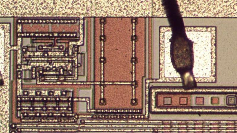
The focus of [Ken]’s exploration of the venerable chip is the charge pump, a circuit that he explains was used to provide a bias voltage across the substrate of the chip. Early chips generally took this -5 volt bias voltage from a pin, which meant designers had to provide a bipolar power supply. To reduce the engineering effort needed to incorporate the 8086 into designs, Intel opted for an on-board charge pump to generate the bias voltage. The circuit consists of a ring oscillator made from a trio of inverters, a pair of transistors, and some diodes to act as check valves. By alternately charging a capacitor and switching its polarity relative to the substrate, the needed -5 volt bias is created.
Given the circuit required, it was pretty easy for [Ken] to locate it on the die. The charge pump takes up a relatively huge amount of die space, which speaks to the engineering decisions Intel made when deciding to include it. [Ken] drills down to a very low level on the circuit, with fascinating details on how the MOSFETs were constructed, and why eight transistors were used instead of two diodes. As usual, his die photos are top quality, as are his explanations of what’s going on down inside the silicon.
If you’re somehow just stumbling upon [Ken]’s body of work, you’re in for a real treat. To get you started, you’ll want to check out how he found pi baked into the silicon of the 8087 coprocessor, or perhaps his die-level exploration of different Game Boy audio chips.


The point was (a) not to waste another pin for the supply voltage and (b) reduce the amount of support circuitry. The TMS9900 (also a 16 bit CPU, but a couple of years older) needs a +5, -5 and 12V rail in order to work. This made it significantly more expensive to build a computer using one.
Now I see why -5 volts… but why some chips also needed +12V?
Old style NMOS logic. The logic gates used an NMOS (N channel enhancement mode FET) as the load for the switching transistors and to make these conduct you need to tie the gate to a higher voltage than its source. However, with an enhancement mode FET this is a problem, because you typically need around 8-10V on the gate to make the transistor fully conductive, at 5V it would be just barely starting to conduct and such gate would have very poor output driving ability. So +12V rail was used for this instead.
Later versions of NMOS started to use depletion mode N-FETs for the load transistors, those are normally conductive and you close them by applying low voltage on the gate. So the +12V rail was not needed anymore, except for peripherals (such as UARTs, which used +12/-12V for RS232 or disk drives).
Ehm, 7905 (7805 is only a positive regulator and won’t work as you described) can’t produce negative voltage out of a positive one. If you want both positive and negative rail (which is the case here), you would need a bipolar supply already and the 7905 will only regulate the negative rail.
Another thing is that regulators like 7805/7905 need a certain minimal current to start to regulate, which might not be there if the regulator only provides bias voltage. Also, these regulators have around 2V dropout voltage, so you would need to power the IC with cca 7-8V for it work. And, finally, efficiency … Charge pump is a switching regulator, 7×05 are linear and waste all the extra energy as heat.
So nope, they couldn’t have done it like that.
That’s only true if you don’t need significant current to ground, since “ground” is at +5V over your circuit’s *actual* ground. There’s a reason the 79xx regulators exist instead of everything being 78xx, and that’s because it’s kludgy and improper to use 78xx that way.
What Jan said…
But I’m surprised they didn’t just source/make a separate die with it on and package them together.
Wtf no multi die assembly is much more expensive.
Ahh.. the olden days of 3 supply rails to use one digital chip.
4 rails if you wanted to communicate with anything outside, because you *were* going to do that over RS232.
And we haven’t touched biphase clocks yet.
Brings back memories. Which is why I’m going to go start daydrinking now.
Thank god we rationalised it into only needing, +5 -5 +12 -12 +3.3 and +5VSB with ATX…. eh whoops, maybe ATX 2.0 where it dropped -5…
Intel is currently working on introducing a new standard for power supplies that is basically +12v only, with any other rails being generated on-motherboard. Some servers (including AMD based ones) are already using it IIRC, so now it just needs to be adopted by consumer boards.
DDR5 is also moving voltage regulation onto the DIMM per its spec.
Granted there are still like 5-10 different rails but other than +5V for USB and non-NVMe drives most of them are generated on and never leave the motherboard.
All those people who overbuy and “invest” top price into a PSU for them to last 20 + years got to be aware PSU is still revolving. I settle for a good enough PSU that would 7-8 years.
Still not sure what’s the point on the consumer ATX. Is this a forced upgrade?
My $60 (discounted) PSU already use non-isolated DC/DC from 12V i.e. It has feedback at 12V and decent load regulation at 12V. There is no space saving as the board space for the displaced voltage rails will be larger than the space saving on the connector footprint.
Think the oldest I’ve got that’s still useful for newer machines is an Antec that’s about 15 years old. Before that they had all the beef on 5V and 10A on 12V isn’t really enough for much grunt in a CPU, never mind a GPU too.
From what I understand most of the voltage rails are generated from the 12V anyway. I think the only one that is still used from the PSU is the 5V rail and even then with enough USB ports it might not be able to reliably source the power so it could also possibly be generated from 12V as well. Plus with DDR5 moving the memory voltage regulators on-DIMM that frees up some room for 5V regulators.
Prices are definitely going up on parts though.
Traditionally the voltage feedback is from the 5V rail and the 12V is just an auxiliary winding. As CPU, GPU became more power hungry, the bulk of the power moved from 5V to 12V, this affects the regulation. Like I said, my $60 PSU already have 12V as main rail and its regulation is excellent.
One of the things that people forget is that if the 5V generation (for USB, SATA) are moved to the motherboard. Not only you’ll need the extra board space for the 5V generation, but probably to have an extra connector (board space+ new pinout) for the 5V and 12V output for the SATA.
To be honest, I don’t trust the MB vendors to do the right thing any more. They spend more time adding RGB and big block of plastic than using real heatsink with proper fins. PSU at least have some airflow where it is needed.
This is produce more waste – PSU that would have been reused are now land fills. It is not like anything really changes as the rails are still needed.
The DDR5 supply isn’t anything comparable to the 5V as the wattage are much smaller. The 5V still have to power all the USB port plus whatever number of the SATA drive vs some memory sticks. It’ll use more space than what’s moved off.
Look for an original 2516 EPROM in some arcade or other “antique” equipment. Not the modern EEPROM version, but the 8 bit parallel UV erasable type.
Visible through the erase window is a second tiny chip next to the memory chip with its own bonded wires. I once, decades ago, confirmed that that was a charge pump for the negative substrate bias. You can see it without having to disassemble the chip.
That was one of the first single voltage EPROM chips I used in my CDP1802 first computer as a monitor/BIOS. If I remember correctly (it was over 30 years ago) the 2716 version from TI needed a negative supply, which I was reluctant to add to my sprawling wirewrapped machine.
I have faint memories from 1990 of debugging a CPU board I had designed that used a lot of programmable logic devices in PLCC packages (square plastic lumps with the legs bent under). These packages have extra little metal nubs at the corners, which I found had -5V on them. This was confusing until I realized that they’re connected to the substrate, and are there for mechanical rigidity while the package is molded. The data sheets don’t mention them, of course, since they’re not connected to anything external.
There shouldn’t be a need for a -5 volt bias.