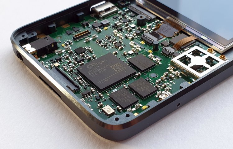
Recently, [Bunnie Huang] announced his Precursor project: a spiffy-looking case housing a PCB with two FPGAs, a display, battery and integrated keyboard. For those who have seen [bunnie]’s talk at 36C3 last year, the photos may look very familiar, as it is essentially the same hardware as the ‘Betrusted’ project is intended to use. This also explains the name, with this development kit being a ‘precursor’ to the Betrusted product.
In short, it’s a maximally open, verifiable, and trustworthy device. Even the processor is instantiated on an FPGA so you know what’s going on inside the silicon.
He has set up a Crowd Supply page for the Precursor project, which provides more details. The board features a Xilinx Spartan 7 (XC7S50) and Lattice iCE40UP5K FPGA, 16 MB SRAM, 128 MB Flash, integrated WiFi (Silicon Labs WF200-based), a physical keyboard and 1100 mAh Lio-Ion battery. The display is a 200 ppi monochrome 336 x 536 px unit, with both the display and keyboard backlit.
At this point [bunnie] is still looking at how much interest there will be for Precursor if a campaign goes live. Regardless of whether one has any interest in the anti-tamper and security features, depending on the price it might be a nice, integrated platform to tinker with.


very nice. I hope they flip the antenna connectors to the back of the board at some point.
Perfect device for the paranoid.
If JTAG pins of the FPGA are exposed, it is not easy to do a dump of the memory (flash and ram)?
Xikinx devices have efuses that permanently disable JTAG if you want that. They also support encrypted configuration bitstreams with either keys in efuses or keys in battery-backed RAM.
I think in this case you explicitly *don’t* want that – the whole idea is that there is no ‘secret’ hardware. If the FPGA is programmed with an encrypted blob, why even bother?? You should be able to read it out and verify that it matches the binary you wanted to put on there.
Just guessing, but I think the idea is that it’s YOUR blob, encrypted with YOUR key.
Parandroid :-D
This looks like an extremely fun project (although I would have preferred if there was a cellular modem as well), and I’ll definitely consider supporting it. Making it useful will probably be a lot harder than making it fun though!
I’m really curious what exactly is in their reference design for the XC7S50 part if they’re already at 80% utilization with a single RV32IMAC core in it – I don’t think I got close to that using an XC7S35 for a Cray J90 SoC I made (and that had full double-precision floating point!).
Not looked in depth yet but it looks like its got the hardware access and options available to talk to the cellular modem if that is what you want to do.
I’m intrigued by it too, but as you say making it useful… A fun challenge and a great excuse to really try and learn the FPGA world.
It’s got four crypto accelerator cores, including a 256-bit wide Curve25519 engine. Those take most of the space.
Ah, that makes sense then. Are you allowed to comment on the target price for the crowdsupply campaign?
So, this isn’t going to need an off-site server that could be shut down like the Chumby?
Pretty sure the point of the Chumby was that while it used someone else’s server, it didn’t have to.
Exactly, I use my original leather-clad Chumby with a hacked up copy of Zurk’s Offline Firmware for the Chumby.
I got burned by Chumby. So I’m not jumping down that Bunnie hole again.
Anybody know if the memories are connected independently as 2x8MB or is the bus shared with just unique CS lines?
Even 64 MB of DRAM would make this project way way more interesting to hack on to me. I might still back it, but will always lament what it could have been.
Looks really well developed/designed FPGA platform already, as was the novina laptop, I’d be interested in one, pending cost and a critical mass of users forming a community around it, i know that’s a chicken and egg problem, but perhaps partnerships with established players, adafruit, sparkfun, arduino, teensey, to push this not necessarily as a product, but as a de facto standard for an open FPGA/RISC V dev device. The Arduino Uno or ESP boards were successful because of cost, community, and of course the software tooling. Bunny never ceases to amaze me with his designs and deserves the attention from the community he’s contributed so much to over the years. Hacking original xbox, SD card hidden controller research, guide to Shenzhen, legally fighting anti-circumvention of the DMCA with EFF, Novina spring to mind.
The hope I had for FOSS FPGA research was the idea of hot core swapping, it was mentioned several years ago at the CCC, referring to the Novina as the dev platform. if was the idea of segmenting the FPGA into blocks that operate independently, for use as a kind of accelerated co-processor, like multi tasking OSes, one could hot swap in cores for crypto, video encoding, or whatever accelerated task was needed, and swap out again for general purpose cores the rest of the time. I hope a platform like this catches on and this idea progresses and it would greatly enhance the power and experience of personal computing
Xilinx has pretty extensive support for dynamic partial reconfiguration. They use it in a variety of products, ranging from correcting soft errors due to ionizing radiation in space, fast startup for PCIE devices, runtime radio waveform codec changes, self-erasing anti-tamper response, just-in-time configuration of accelerator modules, and more.