For anyone serious about mining cryptocurrency such as Bitcoin, we’re well past the point where a standard desktop computer is of much use. While an array of high-end GPUs is still viable for some currencies, the real heavy hitters are using custom mining hardware that makes use of application-specific integrated circuits (ASICs) to crunch the numbers. But eventually even the most powerful mining farm will start to show its age, and many end up selling on the second hand market for pennies on the dollar.
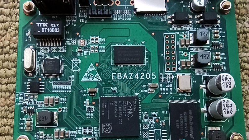
Naturally, hackers are hard at work trying to find alternate uses for these computational powerhouses. While it won’t teach an old ASIC a new trick, [xjtuecho] has documented some very interesting details on the FPGA control board of the Ebit E9+ Bitcoin miner. Known as the EBAZ4205, this board can be purchased for around $20 USD from online importers and even less if you can find one used. Since it’s just the controller it won’t help you build a budget super computer, but there’s always interest in cheap FPGA development boards.

According to [xjtuecho], it takes a little bit of work to get the EBAZ4205 ready for experimentation. For one thing, you may have to solder on your own micro SD slot depending on where you got the board from. You’ll also need to add a couple diodes to configure which storage device to boot from and to select where the board pulls power from.
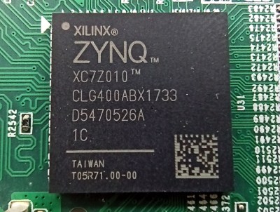
Once you’re done, you’ll have a dual core Cortex A9 Linux board with 256 MB DDR3 and a Artix-7 FPGA featuring 28K logic elements to play with. Where you go from there is up to you.
This isn’t the first time we’ve seen FPGA boards hit the surplus market at rock bottom prices. When IT departments started dumping their stock of Pano Logic thin clients back in 2013, a whole community of dedicated FPGA hackers sprouted up around it. We’re not sure the if the EBAZ4205 will enjoy the same kind of popularity in its second life, but the price is certainly right.
[Thanks to Rog77 for the tip.]


Why are some of the traces by the “EBAZ4205” text wavy?
Most likely the wavy pair of traces are for a very high-frequency signal. It’s probably a signal and return signal over a ground plane. The pair makes a transmission line and needs to be a certain length, spacing, etc. so the impedance is correct.
It is a differential signal with a required impedance. Ddr at this speed is not so critical actually. Routing as differential pair is a must but the length matching not really. But in most cases your pcb tool does it for you so why not.
I just want to comment that this is not exactly correct. DDR operates at a “Double Data Rate” and not deferentially, so while the actual speed itself isn’t the most important, the Data is clocked on both the falling and rising edge of each clock cycle and has to be lined up very close while being measured in the nano-picoseconds range (for the edge slew rate combined with setup-hold time, not data rate). These DDR3 busses are on a zynq 7000 so they’re likely at least 64 wide (maybe 72 ECR) so you have match the data lines, address lines, control lines, length fairly close. with the different geometries of the chips (destination and source). Additionally, you’re definitely going to have some ringing and crosstalk on every line with all these ~100+ signals bunched together in a very small space so you have to keep the lengths matched even tighter to allow more margin for this.
It basically ends up a literal pile of spaghetti trying to keep all the lengths matched but having varying degrees of distances to cover. In short, if you want every marginal card you build to work with every marginal bin of chip (both fpga and ddr), you need to take a very close look at these things. Speaking from experience with Zynqs and DDR4, short of any rf applicaitons, DDR routeing is definitely the most difficult poriton of the design in these cards and getting correct length matching is very important. Additionally, even the most advanced tools only get you most of the way when there’s this many signals in such a small area that you keep having to tweak due to crosstalk issues the tools can’t take into account.
Out of curiosity, do you know of any RF simulation tools that are used when designing these boards, or is it best practice & physical trial and error?
Replying to Rog, I use Hyperlynx at my work along with the rest of the Mentor suite, but most major toolsets have their own sim software associated with them. Unfortunately I’m not familiar with any hobbyist level packages but I’m sure there has to be some out there.
Thanks for taking the time to respond, that’s certainly worth a look :-)
This is incorrect. The purpose is to have the same length of all the traces connecting the DDR chip to prevent timing shift between the lines of the bus.
Impedance matching, RAM is operating parallel interface at high speed. That needs all traces to have matching length so signal is propagated correctly
To have the same length so the signals arrive at exactly the same time without one of them being delayed by longer trace. This is needed for high speed communication with tight timing tolerances, usually CPU/memory bus.
There are some scary PCB design requirements going on around that DRAM chip in the top photo! They continue on the bottom of the board too according to a photo at the link. (And who knows – on inner layers?)
Or am I just being an old fogie because I’ve never laid out a modern DRAM?
The traces are length matched. It is important for all the signals to have the same propagation delay so the signals line up. On the PCB you just squiggle the trace to add length so your shorter traces match the length of your longer runs.
Impedance matching the traces to keep timing and jitter low. Last time I spun a board like this we used the top and bottom layers for the DRAM the inner layers were power planes.
They may share some architectural similarities, but an ASIC can’t be reprogrammed like an FPGA.
This board has a FPGA on it, so what’s your point?
Nobody is suggesting repurposing the ASICs (though it would be nice), this is the FPGA control board for them.
Is there a mining ASIC on there? This is the control board for an array of ASIC cards.
There’s also Antminer S9 control boards that have Gigabit Ethernet and up to 1GB of RAM (apparently some may have less) for $15, also using the XC7Z010 FPGA.
I don’t see any schematics for it though, which makes putting it to work doing other things more difficult.
I bought this board and got this schematics and samples. Did not have time to play with yet.
https://github.com/KarolNi/S9miner_sample
The schematic is accessible through the git link in the article: https://github.com/xjtuecho/EBAZ4205/blob/master/HW/EBAZ4205.pdf. The board itself should be easy enough to use using Xilinx tools. They have free video documentation available on their website last time I checked. Personally I can think of several uses for this bad boy. That pricepoint is cheap.
Biitmain used a BeagleBone running Linux as the network interface for ages. Then a modified BeagleBone for additional ages. I think S9 has one in each unit. 5 year old miners should be free scrap now.
Your comparing RPI type soc’s with an fpga… there’s a distinction here I think you may be missing
Solarflare NICs also go cheap (Ex-HFT/FinTech?) , but I read they use the FPGA as a bump-in-the-wire, and the SDK to reprogram them is quite expensive. Shame, because I have seen previously ten grand boards go for $100.
I am confused, is does this board use ASIC or FPGA? The article starts talking about ASIC then start talking about FPGA on EBAZ4205 miner. It left me scratching my head if I same how missed something in my understanding of ASIC and FPGA. Here is my conclusion. There are many kind of miners. High end miners use ASIC that are not reprogrammable. However EBAZ4205 uses FPGA that can be hacked.
Thanks for the article.
This is a FPGA based control board for crypto coin mining ASIC boards that aren’t included.
The point is that the FPGA control board used in the ASIC miner is being sold for for cheap since it’s no longer powerful enough to keep up with crypto.
This features a dual core ARM microprocessor coupled with an Artix7 FPGA. The board was used to control ASIC miners. You can repurpose the board because you can write your own code to control the FPGA and microprocessors. You just need Vivado.
The fact that ASIC and undocumented FPGA miners exist is a really nasty thing about bitcoin. A computer made today will likely be usable for something for 20 years.
Bitcoin is a constant arms race, and the more money you make, the note hardware you can buy, and the more you need to keep up when everyone else is doing it. PoW can never be efficient. They’ll just increase the work.
You can tack on extra centralized stuff that’s basically a bank to make it work, but the chain itself is an e waste magnet.
I’m glad people are doing something about this though! And that they haven’t gone fully to ASIC miners that becomes trash next upgrade cycle!
They really should just release all documents for all obsolete miners so the previous generation isn’t garbage.
Crypto currencies are indeed mainly generating E waste while also burning currently a fair few GW of power world wide…
Though, in regards to ASIC miners, they are very very common.
The board in the article is just a controller for an array of ASIC miners. (The ASIC minner cards are though not shown in the article.)
And yes, when a new crypto mining ASIC that is a bit faster or more power efficient comes out, then the old ones tends to largely be junk….
If I recall currently, someone thought of the novel idea of using “old” AISC mining chips for a space heater. But that didn’t take off due to its high price, and laughable mining speed making it impractical for mining to be a notable feature.
There is even ASIC miners the size of USB thumb drives, as can be seen here: https://hackaday.com/2013/06/23/turning-the-raspberry-pi-into-a-bitcoin-miner/
(And yes, that raspberry pi miner’s ASICs are likely laughably obsolete in the crypto world…)
Could at least some mining ASICs be repurposed into PRNGs? Or more generic hash crackers?
Also, cheap used Bitcoin miners are great for those who overprovisioned their solar and those who get electricity at a fixed rate in a dorm or apartment. Although used servers might be a better bet since those have uses beyond mining.
Personally, the altcoins I prefer to mine are the ones that can be profitably mined using cheap tablets and smartphones. There’s just not many of those and even fewer that are still profitable to mine, although one – Swagbucks – has lasted far longer than I expected.
Id wouldn’t suspect that most mining ASICs have kept “post mining” applications into consideration at all to be fair.
Mainly since it adds additional logic into the signal flow in the device.
This will both lower power efficiency. (Ie hashes/watt)
And also lower peak performance. (ie, hases/second)
Two fairly undesirable things as far as miners are concerned.
Though, if such additions would make the chip usable for other things than just mining.
Then it at least wouldn’t be literal e-waste at the end of its life.
This is though true for most accelerators aimed squarely at one specific task.
But it would be nice if one could use a “mining” ASIC for file hashing, key generation, and general Pseudo random number generation. (Though, for the last thing, a couple of web cameras looking at lava lamps and hashing the images captured can provide a lot more “true” randomness. (Obviously a reference to Tom Scott’s cloud flare video… And Hack a Day even has an article about it: https://hackaday.com/2018/01/04/the-grooviest-random-number-generator-ever/))
In my own opinion though.
Crypto currencies are nothing but an overhyped waste of resources and energy, for what is frankly worthless logs of transactions.
I hope you drive an electric car or bicycle to work (or telecommute as many do nowadays) since my Swagbucks mining setup used fewer watt hours per $ made than driving 20 miles round trip daily to a $50/hour job in a Prius, even under the very unrealistic assumption that the workplace uses no energy.
That said, the more promising route to energy efficient mining is to make the mining do useful work. Curecoin and Foldingcoin are the ones I especially like since they mine using biomedical research.
Probably not. The hashing done in the ASICs is completely optimized for the specific Bitcoin use case. For instance, the result of the hash will be checked internally, and then thrown away if it doesn’t meet the difficulty level.
Looks like ebay.cn saw this article, loads of them listed as zynq fpga dev boards! Still dirt cheap.
They have been listed as Zynq devboards on eBay and Aliexpress for weeks. My board arrived two days ago.
I bought the cheaper one without presoldered µSD slot. The slot, a 1×4 header, and a 2×7 header were provided in a separate bag.
Can the FPGA be re-programmed without a high dollar software package?
yes
Vivado is free to download. I believe there are limitations to the free version however.
The Pano Logic G1 board only has 16k logic elements, but the G2 has 100k to 150k, which puts this control board to shame.
The nice thing about this control board is that it has an ARM processor inside it.
Pano logic G2 use a spartan6 LX100/150 which is only supported by one free ISE version, running only on win10 pro. Or with licence, in this case you probably don’t care about board price.
The “win10 pro” only ISE is actually a VM running Linux. Many people have copied the files to Linux and run it natively. For example: https://www.thanassis.space/myowncpu.html
can i programm this board with j-link segger or i need some thing else?
in case someone finds himself in the same situation as I (bought the T9+ and didn’t get any doc regarding it), Antminer T9+ has the same pinout for PS side as Antminer S9, so example project from S9 can be used for Antminer T9+ (S9 files are provided above in KarolNi comment from November 19, 2020 at 12:17 am). As for the PL side I’m still trying to sort it out. As far as I checked, J8,J7 and J6 has the same pinout, but the difference is that T9+ has additional resistors and clamping diodes (probably for Zynq IO protection). Also J2, J3 and J4 are tottaly different, so It’s pinout still needs to be determined.
Thanks, also ordered a T9+ but haven’t started yet ..
Is there a JTAG or UART interface?
Yes, J7 is UART and J8 is Jtag, just solder some headers and enjoy
To have the same length so the signals on both (or multiple) lines arrive at the same time. This is a requirement for high speed signals with tight timing tolerances.
I will implore you all to work with the professionals….I got my 3.5 btc completely in my wallet this morning and I want to thank the greatest bitcoin miner prof sydney for making this happen. I cannot keep calm anymore because i got it completed in my wallet and the funny thing is that i have not emailed the prof yet but i am so surprised and i know many people might need this to be financially free. I am happy to join the mining team as this is my best decision so far this year. contact him here bit.ly/3UbOAbr