SD cards have long been a favorite with microcontroller hobbyists. Cheap, readily available, and easily interfaced, they remain a staple for small projects that need to store a lot of data. Now, they’re available in chip form! These are known as SD NAND parts that emulate the SD card interface itself.
[LadyAda] recently gave them a test-drive after spotting a tweet from [Greg Davill] (who we’re familiar with thanks to his excellent LED cubes). The devices are manufactured by XTX Technology and available from LCSC in a range of 1, 2, 4, and 8 GB sizes. [Ivan Grokhotkov] also illuminated a similar device from another maker in a reply to [Greg’s] original tweet, so there may be more sources out there.
These chips come in standard LGA8 surface mount package and can be easily soldered to a board, offering mechanical and manufacturing benefits versus using a normal SD or microSD card in a slot-type connector. Also, unlike other SMD flash memory parts, they handle all the file system details and wear levelling for you! With the inflation of SD card sizes, it’s also difficult to find these on the shelf in normal cards these days.
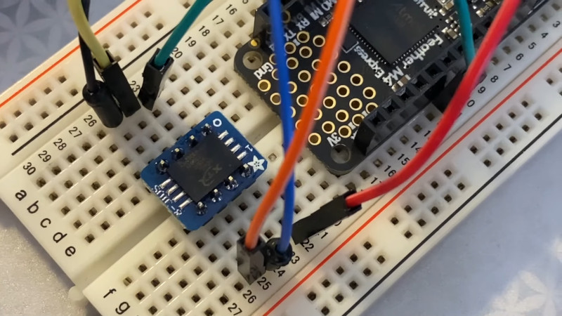
[Adafruit] plan to have a breakout for these parts out soon with a level shifter included for ease of use. We can imagine these chips finding their way into all manner of datalogger projects, since they can be ordered with other parts and permanently soldered into a design. If you’ve got a particularly good idea where these chips would prove useful, sound off in the comments. Video after the break.


How are they different from eMMC, other than the simplified pinout?
eMMC has a 8-bit parallel bus vs SD SPI x1/x4.
here is a very long pdf article about eMMC. JEDEC specs are no longer available to public
https://www.cnx-software.com/2019/08/16/wear-estimation-emmc-flash-memory/
opps. regular web page. not pdf. (I was making a hard copy in pdf)
eMMC can work just like SD using 4bits, https://forum.armbian.com/uploads/monthly_2019_11/RaspiKey.jpg.39195bcc24cd981249136f1e0400f10c.jpg
In fact, both SD cards and eMMC chips can work in even 1-bit mode.
Of course you still need the other “control” wires and vcc & gnd, but I’ve tested it myself with a OG Raspberry-pi with the 26 pin header having all control pins broken out for the second SDIO “port” but only 1 usable “bit” of the data lane hooked up to the second SD card.
And also recovered files of the eMMC of a first gen Sony Xperia Compact with some fiddly soldering to the bare essential points so I could do a dump due to dead SoC.
Fancy shit.
Sweet. Now I have an urge to extend my RS232-TTL project to be an RS-232 SD card adapter :-D
Apart from the package being a fiddly fine-pitch BGA, eMMC cannot be accessed via SPI mode (as dumb as it sounds, this is written into the eMMC specification!).
If you are buying an SD NAND instead of a regular SPI EEPROM, you are not going to use the SPI interface anyway.
Uhh… exactly *why* would you think that? SD NANDs have ludicrously higher densities than SPI flash, because they’re NAND instead of NOR. But most microcontrollers don’t have a hard SD interface, while they do have hard SPI.
The RPi 4 has an EEPROM. Why not stick one of these on as well?
The compute modules ship with eMMC. The EEPROM is just for booting.
That looks great ! however this removes one biiig advantage of discrete-removable µSD cards : you can take it and plug it into your computer to format/copy/write/edit…
Otherwise, one direct application would be with sound players/recorders such as https://wiki.dfrobot.com/DFPlayer_Mini_SKU_DFR0299
Super a sd card I cant remove and stick in my computer … How is this different than a rom with anfilesystem?
Did you read anything? It handles wear levelling automatically, and it uses the SD interface, so it could be used with a ton of existing applications alrwady
Technically so does SD cards of any variety.
The key being how crap the controller on the card is (in terms of prolonging lifespan of the raw flash memory) and the actual quality (and quantity in the name of redundancy) of the raw flash memory.
Or long story short: except for some shyster big brands, you get what you pay for.
Only place i can see this being preferred is applications requiring conformal coating or is exposed to extreme vibrations that could break a micro-sd socket.
yes welcome to a decade ago, thanks for playing
For 3 usd you can get 16-32 GByte sd cards, the lcsc linked product is 4 Gbit (512 MB) for he same price, sd card socket is around 0.15 usd. And you can change the card.
But sometimes that extra functionality causes extra “customer service” for the warranty breakers who have no skills. In these cases, it can be cheaper to pay extra for “permanence.”
Plus you get a known performance profile. I’ve ran into many name brand micro sd cards that just flat out don’t work with a product (dash cam) due to shenanigans happening behind the scenes on the internal controller. This absolutely impacts your customer service cost
So this is why Samsung & Apple charge so much more than SD prices for storage upgrades.
And the planned obsolescence when the storage wears out.
You know, the irony of “planned obsolescence” is that when that really became a pop-culture buzzword, it was directed toward the cars of the 1950s/1960s…which were pretty much built like tanks and many of which are still around.
But year, don’t put this in any gadget you need to work 20 years from now–then again that is not a concern for many devices.
“…it was directed toward the cars of the 1950s/1960s…which were pretty much built like tanks and many of which are still around.”
Oh my sweet summer child. I grew up near a GM plant – those cars were absolutely built to a price and were meant to be replaced every three or four years either by incompetence or conspiracy (your choice). 100,000 miles was a lofty goal and often not attained before the rest of the structure disintegrated. The engine designs were antiquated and their efficiency was laughable at the very least, as were the corporations that produced them.
By contrast my current truck has 103,000 miles on it, will go many more and has run flawlessly from day one.
Look at the Tesla issue with the non-removal flash that wears out. IIRC its in their tablet/user interface.
None of my 1960’s cars made it to 100,000 miles. Yes, they were built like tanks: unnecessary, excessive metal in lots of places and intended to go a short distance before heavy maintenance and repair required. Modern cars still look good and work well after 250,000 miles: very few of them are completely rusted out and most of them have their original engines.
My 1952 Jeep broke the starter retract spring about every 20 times I started it. It needed an engine rebuild at 43,000 miles. I think I spent about 1 hour working on it for every 20 hours of driving it. I can’t remember how many times it stranded me when a u-joint failed, the clutch pivot broke, the shift lever snapped, the frame rusted through, the suspension pivots rusted out… The heater had one speed and only blew on my feet and then the cable housing for the hot/cold broke off the back of the dashboard so it no longer worked, and every time I pushed the throttle down the windshield wiper (singular) stopped working and I had to turn it by hand via the lever provided for exactly that situation.
Cars back then were *terrible*. Cool, fun, that’s why I still drive one, but modern cars beat them in every single quality metric save appearance.
And if you need to service one of these 2020 cars you need to break out the ODB2 cable and the vendors software you needed to download from some shady Russian hacker forum. ¬.¬
I remember the first real computer upgrade I did as a kid was installing a 2gb harddrive circa 1997. Now that capability is in an SMD chip for $2.52.
The computer that harddrive went into was out of use by 2001 and lingered in my parents’ garage around for a few more years before being scrapped for misc parts–and that was probably a long life for a machine from 1994.
I remember paying $205 to upgrade from a 40MB HDD to a 540MB HDD and paying $80 for 4MB (4x1MB) used SIMM ram chips. It’s definitely gotten a bit crazy how cheap storage is now.
My 1st upgrade was a 10mb HD mounted on a 8 bit ISA card into my 8086.
I didn’t think I would ever use ALL THAT storage..haha
Heh.
My first storage upgrade was a pair of 8K chips hanging out the back of a VIC-20.
Meh, if it’s a DFN8, it’s not that bad to remove/replace. Certainly better than a BGA eMMC. An SOIC8 would be nicer for dense stuff but obviously the volume reduction’s important.
Where can you get a reliable (i.e. actually advertized size) 16Gb SD card for say “around $3”?
Actually, I’m a bit more interested in say 1/16th of that size for say 1/16th of the costs. I’ll still buy them if it doesn’t scale completely and costs say 1/8th of the price of 16G.
For embedded systems like dataloggers, 1G is already VERY big, but $10 for the smallest I can get is too expensive….
I can’t find much fault with the 16GB one can get in the Dollarama here for $4 Canadian apart from maybe it’s class 8ish rather than class 10, but you get that kinda spec overinflation with some name brands. EAGET brand, if that’s not Dollarama’s own.
There is already a thing called eMMC which is a bit the same. Although it has more functionality than a normal sd card, the footprint is bigger
Unless you have the setup it seems like the real perk is not having to deal with eMMC’s BGA packaging.
If you do have the appropriate gear or are doing volume production eMMC is almost certainly the better bet, higher performance and a lot more vendors; but it’s nice to have the option of shoving an actual block device into what looks like pretty much exactly the same footprint and friendly solderability of a classic teeny SPI or i2c flash chip.
What will be the speed of write and read ? .. I guess it will be very slow !!
The second brand claims 17MByte read and 4.6MByte write.
How does the power consumption of these chips compare with the standard SD cards?
See datasheet on the LCSC link. 30mA
The datasheet
https://datasheet.lcsc.com/szlcsc/2005251034_XTX-XTSD01GLGEAG_C558837.pdf
is not so promising for power consumption:
Standby Current(*)
20* mA; VDD=3.6V, clock 25MHz
0.2 mA; VDD=3.0V, clock STOP, Ta=25°C
Note:Standby current max20mA with CLOCK 25Mhz only based on100pcs samples
couldn’t find any datasheet for the longsto brand
A niche product as I’ve seen (micro)SD cards that are just soldered to PCBs. Depending on who is selling this, I wouldn’t be surprised if they were actually just old SD cards that were repackaged.
Problem with large SD card storage is that it can’t handle unclean power loss. It can even corrupt the card to the point where it can’t be accessed at all.
Another problem is the impossibility of doing any kind of file system check/repair on a small embedded platform.
Yeah, right–
I’m going to solder in a limited-lifetime memory chip into a product / project.
“…There is already a thing called eMMC which is a bit the same…”.
Yes, there is; and, no, it is nowhere near the same.
When did this brain-dead “out of sight, out of mind” and “it works for me right this minute; not my problem any more” mentality get firmly entrenched with people who are supposed to know better?
***********************************************************************************************
“Originality is no excuse for stupidity.”—Fred Brooks
“I don’t care if it works on your machine. We are not shipping your machine!”–Vidiu Platon
It’s limited *use*. So use it as a golden image backup with a 2:1 SD mux (or just handle the CS pin). Now there’s an easy option to avoid failed updates without costing another interface, and you’ll never see the lifetime issue.
When consumers started not only accepting but actively defending throwaway, locked down, closed ecosystem crap.
Probaby because silicon valley has a thing for apple and their “flowing” kind of mindset where stuff is meant to be thrown away every few years, you don’t expect too much from devices, and private is the one and only concern in tech.
The datasheet has no specs on the endurance of the flash, so I wouldn’t use these devices in anything. By itself, the idea isn’t bad. Lots more devices have SD or SPI interfaces than straight NAND controllers, and outsourcing the raw flash handling to the SD card controller simplifies your own software. Soldering down the memory avoids the contact glitches you occasionally get with card sockets.
However, an SD card literally lives and dies by the quality of the flash memory and controller inside – that’s why you pay so much more for industrial cards than the supermarket checkout line cards, and the manufacturer says practically nothing about either, only that it uses ECC somewhere.
The HaD write-up completely bypasses the major negatives of this form factor: lock-in, planned obsolescence, no right to repair/maintain, on-and-on. Thank goodness it took next to no time for the Commenters here to fill the gaps in the woefully incomplete lead-in article. Or maybe this was a “Stealthy-Ad” for Adafruit and/or XTX Technology? If it was – it didn’t work. Oh and one more thing: “SD” cards have been available as Chip-on-Board” (CoB) lead-bond devices since inception. Yes, they’re even cheaper because there’s no need for a physical outer package or leads. You just squirt a blob of epoxy over the chip after dropping it on the PCB.
Oh great, that’s what I need: How come they cannot be found anywhere?
Sounds to me like the kind of thing you buy by the 10,000
You… really don’t see the difference between a chip-on-board package and a DFN8? Really?
Plus railing about “no repair!” is a bit nuts: obviously a CoB package under epoxy is nigh-impossible to repair, whereas a DFN8 available for pennies is pretty easy.
definitely an ad for the overpriced e-waste/junk rebrander/reseller.
There’s some detail on appropriate applications on https://www.youtube.com/watch?v=pbrAQz0ro0Y&t=2m22s
And while I’m here I’ll throw in an inappropriate use of eMMC: https://www.theregister.com/2020/11/17/tesla_nand_memory/
While we are at storage extensions: is there a way for an Arduino to load executable code from an SD (or other external storage)?
Depends on the arduino, the ATmega based boards can’t run native code from external memory. You can use a interpreter to run some sort of byte code from external memory with the ATmega based boards (slow but possible). I don’t know about the other boards.
Thank you
It seems to be possible to load code from an I²C EEPROM. However, it requires a special bootloader and may be quite slow. Of course, it should be possible to use an SD card in the same way. See this page for more informations:https://mitxela.com/projects/console
Great. Very helpful to see a working example. Thank you.
This isn’t actually loading code externally: it’s completely erasing/reprogramming the flash each time. ATmega flash realistically has over 1M erase/program cycles (it’s rated for far less, but this is from testing) so for *casual* reloading this isn’t a bad option.
I just leave it here:
https://habrastorage.org/getpro/habr/comment_images/db3/e29/c83/db3e29c836311b9fda29d266646a20f4.jpg
besides size what are the benefits of using this over a d.o.m.?
Sdcard have the SPI interface. Disk On Module, if that is what you meant, have PATA or SATA which is harder to use with a microcontroller.
yes it is but there are a lot of companies using a usb dom setup these days which is IMHO just as easy if not easier to interface. Just look at all the dom’s that qnap uses.
I use these ICs in ‘parallel’; that is, one for reading and one for writing; never both. Writing is sequential and per a fixed-size (static data). Power monitors allow buffers and in-progress data structs to be flushed to IC before shutdown. Some of the libraries I use follow.
https://github.com/dirkenstein/SPIMemory
https://github.com/kasjer/saleae_spiflash
https://github.com/PaulStoffregen/LittleFS
https://github.com/littlefs-project
Gb, not GB
If I were to use this, it would be in a removable socket but inside a product that would only read from It at boot up then use it to direct to another storage medium (etc sd card or usb drive)
The ic could be removed but 99% of the time wouldn’t need to.
A lot of microprocessors I’ve seen like for example Broadcom arm cpus in raspberry pi’s mainly boot from sd.
If we could make it boot from a built in device similar to a bios then direct it to any other storage medium, it would be useful for board manufacturers.
I imagine it similar to a commodore era rom chip vs floppy disk
(I am not by any means a tech guru, please correct me if I’m wrong)
An interesting device from solely the perspective of its’ physical characteristics. It is _substantially_ smaller than a micro-SD card, and is something that can be used in a design where you don’t have a chip-bonding machine (referring the comment above regarding CoB and DFN) or access to one (ie: I don’t want to make 100,000 or more).
Anyone know if this size chip (physical size) is available with a USB interface rather than SD interface?
This article is pretty old and I still see that the only places one can buy these parts is on an adafruit board or direct from a few Chinese suppliers.
Why are they not available from mouser, digikey, arrow etc. Why can I not buy from european and US distributors?
Product is ideal for my app, yet why have other manufacturers not started producing such LG8 products?
I can’t find them on any other distributor websites either. Have you managed to find any other products that are similar?
There is no information about the type of NAND Flash used. Is anybody know this information? If there is SLC NAND Flash it is a super product because it is hard to buy an SLC SD card now.
Product List
Capacity Part number Package Size
1Gb (SLC) ZDSD01GLGEAG LGA8 (Land Grid Array) 8x6mm
2Gb (SLC) ZDSD02GLGEAG LGA8 (Land Grid Array) 8x6mm
4Gb (SLC) ZDSD04GLGEAG
04GLGEAG
LGA8 (Land Grid Array) 8x6mm
8Gb (MLC) ZDSD08GLGEAG LGA8 (Land Grid Array) 8×6.2mm
16Gb (MLC) ZDSD16GLGEGA LGA8 (Land Grid Array) 8×6.2mm
32Gb (MLC) ZDSD32GLGEGA LGA8 (Land Grid Array) 8×6.2mm
1Gb (SLC) ZDSD01GLGIAG LGA8 (Land Grid Array) 8x6mm
2Gb (SLC) ZDSD02GLGIAG LGA8 (Land Grid Array) 8x6mm
4Gb (SLC) ZDSD04GLGIAG
04GLGEAG
LGA8 (Land Grid Array) 8x6mm
8Gb (MLC) ZDSD08GLGIAG LGA8 (Land Grid Array) 8×6.2mm
16Gb (MLC) ZDSD16GLGIGA LGA8 (Land Grid Array) 8×6.2mm
32Gb (MLC) ZDSD32GLGIGA LGA8 (Land Grid Array) 8×6.2mm
Hi and hello everybody!
I’ve been struggling during days to find out more information about how to implement such a chip in my project, (or in any project in fact).
I’ve been looking for different ways to get an easy extra memory storage for an ESP32 (or Arduino as the most famous).
I’m really not the only one to look for such a way to add extra (lot of) memory in an easy and “plug and play” way.
In fact, i’ve seen that is a reccurent question, about how to get around SD card limits:
Vibrating environment that can disconnect it, or simply the risk for an user in a finished product to remove it and get access to the data.
This chip seems to be THE answer, but i didn’t find any “tutorial” on how to solder, plug, set, code etc…
I really would like to create a such full tutorial about it, but my knowledge and lake of informations stop me.
The aim is to plug this chip (already solderred in a SOIC-8 socket as the video above shows, and as PICT A) in a kind of PCB 1 (PICT B), which then could be plugged into an USB computer connection.
I made this (uggly) protype PCB 1 by soldering an USB card reader model, and following connections like Drawing_A.
So it could/should appear as an USB storage, and transfer files on it from a computer.
Then, in a second time, unplug the chip from this PCB 1, and plug it into a PCB 2 (final PCB Product), where the ESP32 (or Arduino) is.
By this way, the ESP32 (or Arduino) could communicate with it, as an SD Card (with related easy librairies).
If everything works, this chip/SOIC-8 socket could be soldered into the PCB 2 so it can’t be removed from the finished project, or at least, not in an easy way as an SD card could be.
There are also other options like desoldering the chip from its SOIC-8 socket and solder it directly to the PCB 2 (but what about reliability on data when heating the chip again…?).
Or even better, solder the chip into the final PCB (creating its own SOIC-8 pads) and create tracks from it to some “plugs”, where the PCB 1 could be plugged in with an 8 wires cable just for transferring files. (Drawing_B)
So here are some of my questions…:
Does anyone has already made this? or another way to reach my goal?
Also, do i have to short circuit the switch into the USB car reader?
If i solder the chip directly to my final PCB, i should wire it as an SD card for the USB connection to the computer (via the plug and 8 wires cable), but then i should follow the SPI connections (table on Drawing_A) to connect it to the ESP32 right? (like an SD Card)
For now, i can’t make it appear as an USB storage, probably some soldering problems that i need to fix?
I hope someone around could tell me if i’m right in my drawings, and if this method could work, of if i’m missing something…?
Thanks a lot for your time reading this, and feeding me with some answers!
Frederic
PS: i can’t leave the pictures (so all this litterature is useless…), is there a way to attach them?…Thanks