Atomic force microscopy, laser ablation, and etching with a witches brew of toxic chemicals: sounds like [Zachary Tong] has been playing in the lab again, and this time he found a way to fabricate arrays of microscopic lenses as a result.
Like many of the best projects, [Zach]’s journey into micro-fabrication started with a happy accident. It happened while he was working on metal-activated chemical etching (MACE), which uses a noble metal catalyst to selectively carve high-aspect-ratio features in silicon. After blasting at a silver-coated silicon wafer with a laser, he noticed the ablation pits were very smooth and uniform after etching. This led him to several hypotheses about what was going on, all of which he was able to test.
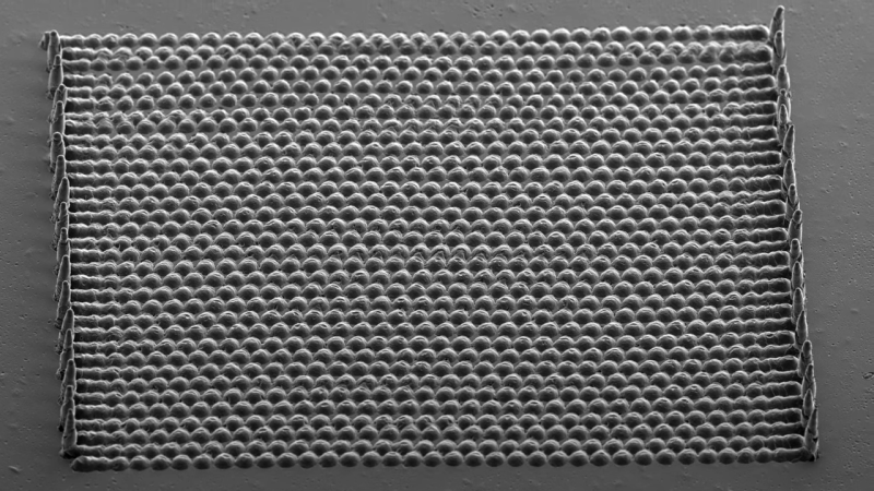
The experiments themselves are pretty interesting, but what’s really cool is that [Zach] realized the smooth hemispherical pits in the silicon could act as a mold for an array of microscopic convex lenses. He was able to deposit a small amount of clear silicone resin into the mold by spin-coating, and (eventually) transfer the microlens array to a glass slide. The lenses are impressively small — hundreds of them over only a couple hundred square microns — and pretty well-formed. There’s always room for improvement, of course, but for an initial attempt based on a serendipitous finding, we’d call it a win. As for what good these lenses are, your guess is as good as ours. But novel processes like these tend to find a way to be useful, and the fact that this is coming out of a home lab doesn’t change that fact.
We find this kind of micro-fabrication fascinating. Whether it’s making OLED displays, micro-machining glass with plasma, or even rolling your own semiconductors, we can’t get enough of this stuff.


My guess: light field optics
Yeah that was my immediate thought as well.
I’ll add this link about “Making Tiny Fresnel Lenses” https://www.youtube.com/watch?v=uf3Y0-6NbjQ Which are much larger at 0.5 mm to 1.5 mm (0.02″ to 0.06″), but still are interesting lenses.
Some Infrared (IR) antenna call for (very) small apertures. Maybe this tech could open up a world of cheaper IR sensors.
Just to further clarify (justify?) my comment…
I read somewhere, years ago, that far infrared (i.e. heat) detectors in nature (bugs/snakes) utilize small apertures.
I would love it if these lenses could be overlaid on a mobile phone screen so that each pixel had a focal point of infinity, so that these old eyes of mine could use a mobile phone without reading glasses. :-)
Been done, but with a different effect. Actual stereoscopic display without glasses. Leia produced the red one phone, and it looks like now a tablet.
https://www.leiainc.com/
Cool. Thanks for that link.
Lots of cool info in that video. Micro-lens arrays have several applications. They are used to increase the efficiency of pixel displays, and, as mentioned above, can redirect light for either stereoscopic or light-field applications. They apply to both displays and image sensors.
I made some 10 years ago these:
https://www.youtube.com/watch?v=qmDPishgLxM
made from a siliconemold, which was made with 1 mm stainless steel balls. lenses are epoxy-resin, 2800 dpi-inkjet-print, glued with epoxy.
Would be nice to have a full write-up of that.