We’ve been following [Vik Olliver]’s progress on the μRepRap project with interest for some time now. The project’s goal is to build a 3D printer that can print feature sizes down to about 10 microns – the same feature size used in the Intel 4004 processor. At the recent Everything Open 2026 conference, [Vik] presented an overview of all the progress he’s made in the last year, including printer improvements, material woes, and the first multi-layer prints (presentation slides).
The motion stage has undergone some fundamental improvements recently. The original XY motion table was supported on four flexures which allowed movement in X and Y, but also introduced slight variations in Z – obviously a problem in a system that needs to be accurate down to the microns. The latest version now uses complementary flexures to maintain a constant Z height, and eliminates interference between the X and Y axes. The axis motion drivers were also redesigned with parallel-bar linear reducers inspired by a pantograph, increasing their usable range from two to eight millimeters.
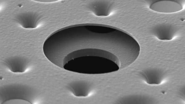
Rather than extruding material, the μRepRap uses an electrochemically-etched needle point to deposit UV-curable gel on the build surface. [Vik] found that a bit of nitric acid in the needle etching solution gave the edges of the probe a bit of a rough texture which let it hold more resin. He started his test prints using normal 3D printer resin, but it turns out that dissolved oxygen inhibits curing – quite a problem for small, air-exposed droplets. Fortuitously, UV nail gel does cure in air, and the next set of tests were printed in nail gel, including the first layered prints (one of which can be seen above, on top of a hypodermic needle). The μRepRap can’t yet print large numbers of layers, but [Vik] did print some hinged parts that could be folded into shape.
There’s much more in the presentation than can be covered here, including some interesting thoughts about the possibility of 3D printing electrochemical memory cells in ionic gel. Near the end of the presentation, [Vik] listed some pieces of related work, including necroprinting and this homemade micro-manipulator.