In this wonderful world of MEMS technology, sensor technology has been downsized and reduced in cost to the point where you can buy a car tire pressure sensor for less than $3 USD on a site like AliExpress. Recently [electronupdate] got his mittens on one of these items to take a look inside, and compare it against his trusty old mechanical tire pressure gauge.
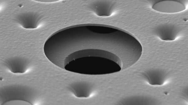
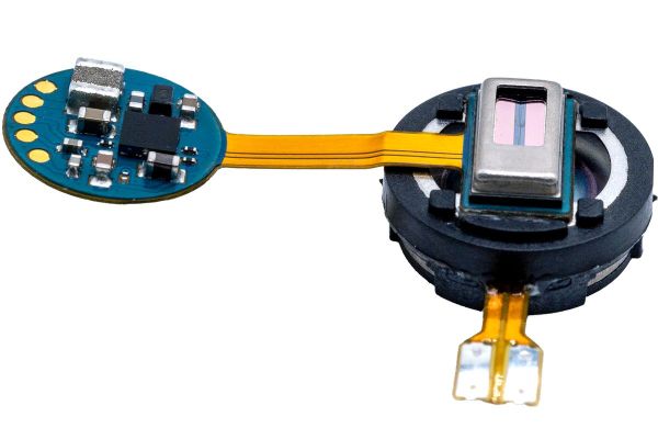
Perhaps unsurprisingly, there isn’t a whole lot inside these devices once you pop them open to reveal the PCB. The MEMS device is a tiny device at the top, which has the pressurized air from the tire guided to it. The small hole inside the metal can leads to the internals that consist of a thin diaphragm with four piezoresistors that enable measurements on said diaphragm from which pressure can be determined.
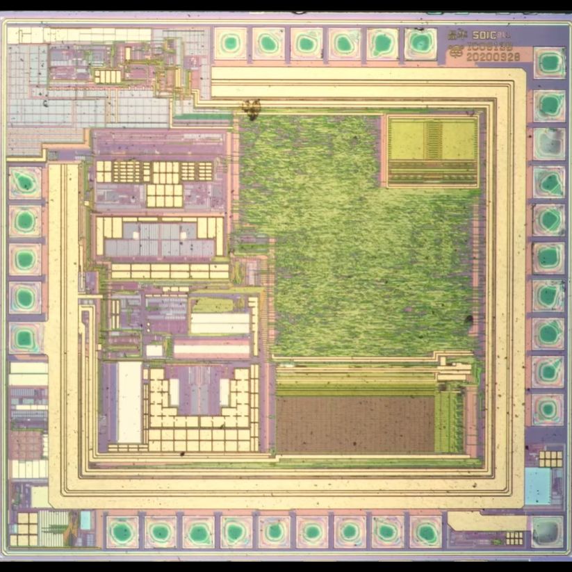
Handling these measurements and displaying results on the small zebra connector-connected LCD is an 8-bit MCU manufactured by Chinese company SDIC. Although the part number on the die doesn’t lead to any specific part on the SDIC site, similar SDIC parts have about 256 bytes of SRAM and a few kB of one-time programmable ROM.
This MCU also integrates the clock oscillator, thus requiring virtually no external parts to work. Finally, its sigma-delta ADC interacts with the MEMS device, rounding out a very simple device that’s nevertheless more than accurate enough for a spot check as well as quite portable.
Continue reading “Reverse-Engineering A Handheld Car Tire Pressure Gauge”