It seems only appropriate that hot on the heels of the conclusion of Hackaday’s 555 Timer Contest that [Ken Shirriff] posts a silicon die teardown of an early version of a hacker’s favorite chip, the 555.
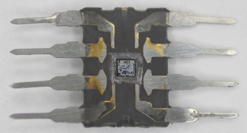
Starting with a mystery chip from January 1973, [Eric Schlaepfer] painstakingly sanded down the package to reveal the die, which he deemed to be a 555 timer. Why didn’t they know it was a 555 timer to start? Because the package was not marked with “555” but rather some other marks that you can see in the blog post.
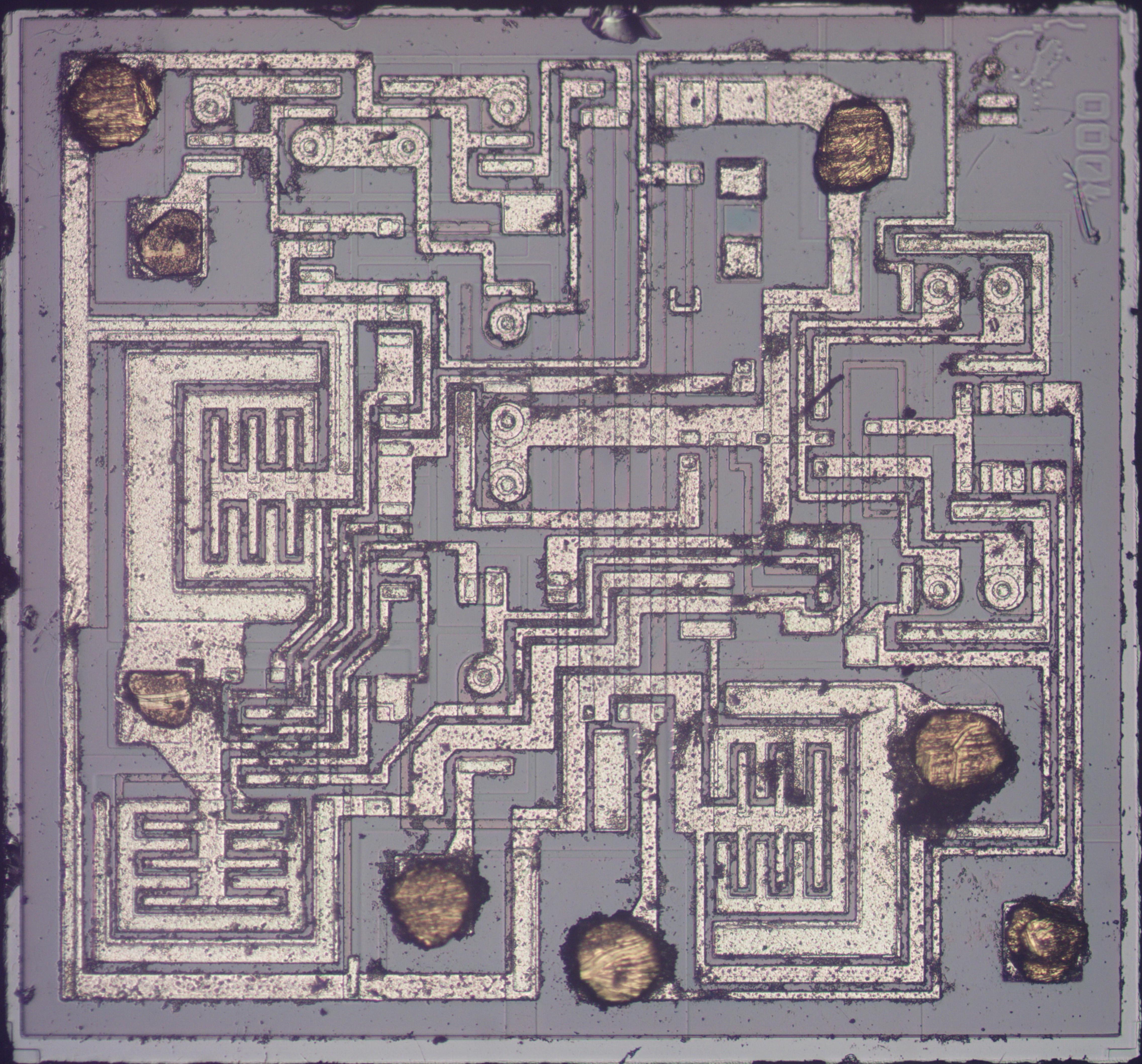
In addition to a great explanation of how the 555 works in general, [Ken] has taken a microscopic look at the 555 die itself. The schematic of a 555 is easily available, and [Ken] identifies not just sections of the die but individual components. He goes further yet by explaining how the PNP and NPN resistors are constructed in silicon. There’s also a nice and juicy bit of insight into the resistors in the IC, but we won’t spoil it here.
Be sure to show your love for the winners of the 555 contest, or at the very least check out the project that took the stop spot: a giant sized 555 that you don’t need a microscope to see inside of.


The description of the operation of a current mirror is wrong.
Quote : “Since both transistors have the same emitter voltage and base voltage, they source the same current”
This is not true, identical transistor can have different collector currents for the same base voltage- emitter due to variations from one transistor to the next even on the same die. It’s no a huge difference but it’s what a current mirror is used to avoid.
A current mirror fixes the total current for both base emitter junctions of the differential pair so that for one to go up the other must go down, this is the “mirror” effect. As the collector current is a product (HFE) of the base emitter current the differential collector currents are also mirrored.
So instead is looking at Vbe of the three transistors think of it this way –
If I name the three transistors TR (reference), TD1 transistor 1 of the differential pair and TD2 transistor 2 of the differential pair. And RR the reference resistor. Ibe = current base emitter, Ic collector current
The current through the reference resistor = TD1 Ibe + TD2 Ibe + TR Ibe + TR Ic
TR Ic is fixed by RR so the the total addition of TD1 Ibe and TD2 Ibe is also fixed meaning that any increase in one causes the other to decrease. This is why it’s called a “current” mirror and not a “voltage mirror”.
There are a number of ways to do this but this way works at lower voltages as there is no Vbe stacking and uses less resistors. However it is a little less accurate
The link for “giant sized 555” is dead.
It is also dead in the page linked (“winners of the 555 contest”).
Works for me. Try again?
You could have done that with a single 555…
hahahah to die for lmao i get it
Admittedly, I hadn’t read it the way it was intended. I thought is was the resurrection of the old fellow.
Ken Shirriff is national treasure.
The old ‘triple-nickel’ will live on forever, like the rider on the MTA…
I was looking at the schematic of an old computer I once had. Here it was called a VIC-20, I think there it was called a Commodore 16. It was made before the Commodore 64.
It had a 555 in it!
We should go hunting them in the wild just to see where they’re hiding!
It was called a VIC-20 everywhere.
The Commodore 16 was a whole different device, although in the same box (but dark grey instead of white). It was a newer design than the Commodore 64, more capable in some areas, but decidedly less capable in other areas, which caused its death quite quickly.