
I’ve had a fairly varied early part of my career in the semiconductors business: a series of events caused me to jump disciplines a little bit, and after one such event, I landed in the test engineering department at Philips Semiconductors. I was tasked with a variety of oddball projects, supporting engineering work, fixing broken ATE equipment, and given a absolute ton of training: Good times! Here’s a story that comes straight off the oddball pile.
We needed to assemble a crack team of experts and high-tail it to deepest darkest Wales, and sort out an urgent production problem. The brief was that the wafer probe yield was disastrous and the correlation wafer was not giving the correct results. Getting to the punch line is going to require some IC fabrication background, but if you like stories about silicon, or red-bearded test engineers, it’s worth it.
Integrated Circuit Design and Testability
The naïve IC design is one that forgoes testability in pursuit of die area, development time and some misplaced notion of simplicity. I cannot say how many times I’ve come across stories from the past where a new startup proudly makes silicon, but has almost no testability features and they get really hammered when trying to ramp up production.
The chip may be ‘right by design’ in that it is targeted correctly to the fabrication process, and on the bench, the product validation process may show it is within specification and appropriate for the customer’s end application. However once that’s done, we need a verification process to ensure the chips going out the door adhere to that specification, under normal process variances, and they are defect free. See this interesting guide from NASA about this important distinction.
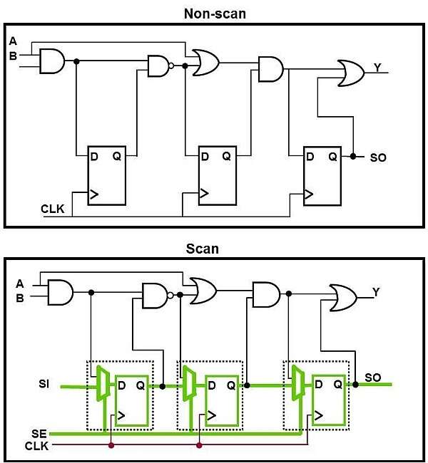
The test engineer’s first port-of-call is the concept of Zero Defect Testing, which relies on design support known as Design For Test (DFT.) This basic guide will serve as an introduction to these concepts for those interested.
These testing methodologies require functional changes to the digital parts of the design, by a DFT engineer. They are almost always automated by dedicated tools as part of the digital synthesis flow, with the test patterns needed to activate ‘scan test mode’ generated by a special ATPG (Automated Test Pattern Generator) tool. This analyses the gate-level netlist of the IC and figures out how to perform the required structural tests. An example of this, that i’ve used in the past is Synopsys Tetramax. There are many, many variations on this test scheme, such as Logic-BIST (Built-In Self-Test) but that’s a subject for another day. Anyway, the goal here is to get the test patterns needed to feed into the test development process, further down the line.
The IC Production and Test Process
Once the IC design is completed, the thing needs to be manufactured. This is done in hugely complicated, immensely expensive facilities, hereafter referred to as the ‘fab’, in a handful of locations around the world. Companies like TSMC, SSMC, or Tower will manufacture your design on a contract basis, shipping wafers off to wherever they need to go to get tested and packaged up.
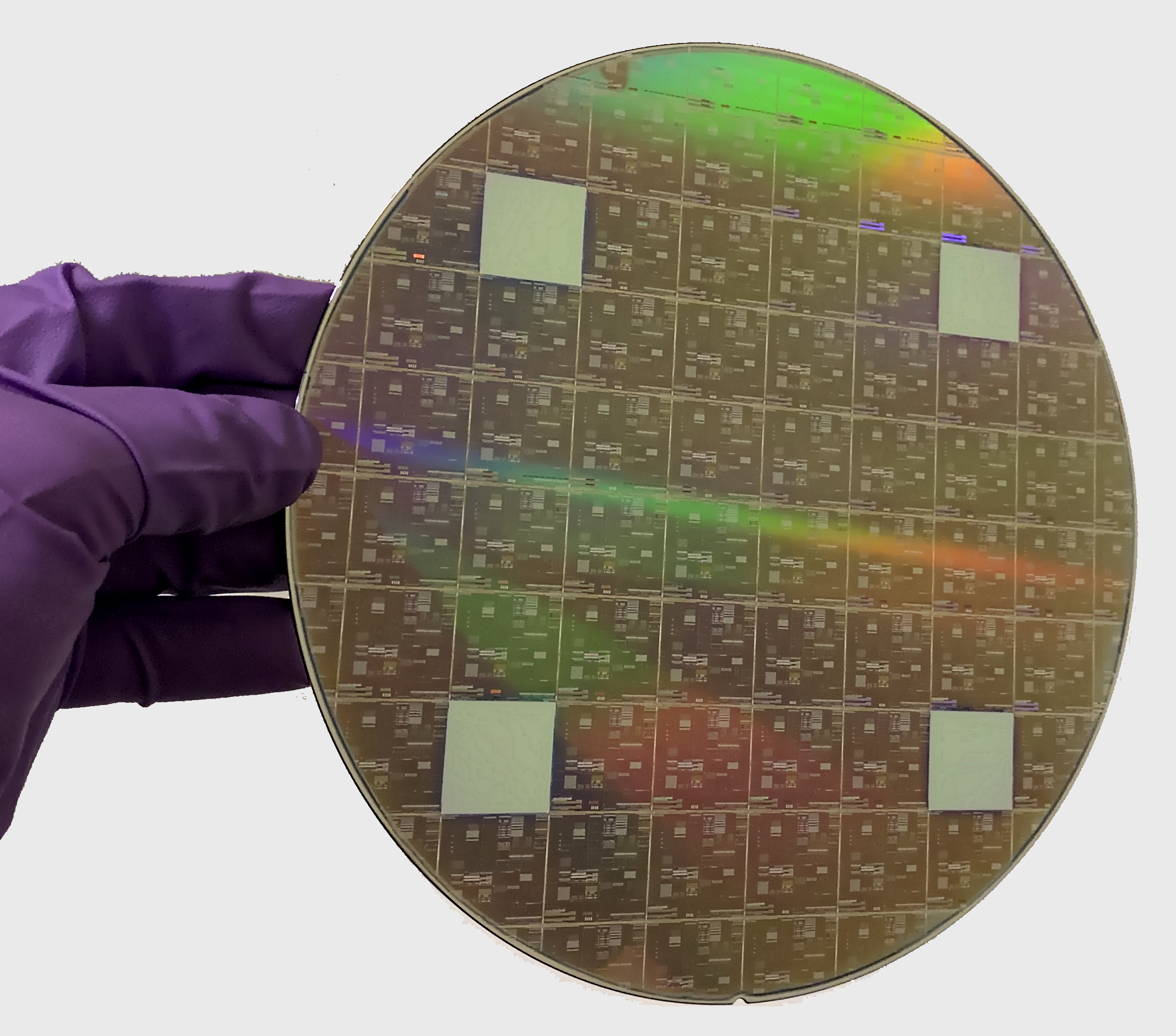
Wafers are shipped out in a plastic ‘boat’, typically 25 at a time, to test-and-assembly facilities all over the world, where they optionally may be tested, then sawn up and packaged. Each wafer will have hundreds or thousands of identical copies of the device, stepped on a rectangular grid over the surface.
Depending on the assembly process, what happens next will work in different ways. Older or simpler designs may just have a simple pad ring surrounding the core of the chip, with metallised contact areas for each connection (called ‘pads’). When packaged, the freshly sawn (or ‘singulated’) die will be glued to a lead frame (a metallic scaffold) before gold (or copper, lately) bond wires are attached between this leadframe and the chip pads, using a wire-bonder machine. The whole thing is then stuffed in a mould and plastic is injection molded around it, before the packages are singulated ready for ‘final test’. Many things could have gone wrong up until this point, so it is critical to test the packages before they are packaged for distribution.
From a test perspective, the wafers will undergo testing as they are processed by the fab. There will be a number of special test dies dotted around the wafer, mixed in with the application dies. These are referred to as Process Control Monitors (PCMs) and are used by the fab internally to measure wafer quality and ensure that the fabrication process is within specified parameters (hence ‘process control’). Select PCM data are delivered to the end customer by an automated process to be accessible by the product engineer (engineer in charge of product manufacturing) if they need it. Once the finished wafers are shipped out to the test house, they might undergo wafer probe testing. If the package cost is low, then the yield impact of not testing before packaging could be low enough that it is not being economically viable to test before packaging. We call these ‘blind assembled’ packages, and so long as the ‘final test’ is good quality, we can be sure the customer will get fully working, in-spec devices. However, if the package is complex, and expensive, wafer probing becomes necessary, and of course, if the product is a Chip Scale Package (e.g. flip-chip) there won’t be a package (or a lead-frame for that matter) as such, just a bunch of solder balls stuck onto the RDL (redistribution layer) but that’s a different problem.
The general plan is to use testing at a variety of points to improve overall quality, by weeding out bad wafers (PCM data) bad die (wafer probe) and then packaging up the good die, before a final quality check. At either of the latter stages product may also be speed/performance graded (or binned) for different final specs. It all depends on the product. What tests are done at which stage also depends on a multitude of factors such as test feasibility with the available ATE platforms, and the expected failure rates vs cost of test. Test-cost economics and subsequent planning is a tricky subject.
ATE Systems
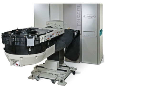
So let’s talk about the tools of the trade. Automated Test Equipment (ATE) is a bit of broad term, but we’re dealing here with dedicated IC test platforms, so that narrows the scope a little. The target platform was the older Teradyne Catalyst system. This machine is an absolute beast, physically huge and heavy, and sucks 3-phase power like its going out of fashion.
The so-called mainframe box, contains big power supplies, support circuits, and waveform sources (if RF is installed) is the size of double-wide US-style refrigerator, but weighs in at a couple of tons. This is attached via an umbilical to the test head. This last bit is the business end, containing the test electronics, local power supplies and is where the tester interfaces to the application.

The idea with these platforms, is that rather than designing a custom test rig per product with a full suite of equipment tied to the requirements of the device, you can design the chip to be testable to within the capabilities of a general purpose platform, then you just need to configure one with enough resources to interface with your device, in its test modes.
A typical ATE test head will be a large box about the size of washing machine (but likely weighing much more) containing some really expensive electronics. They’re usually arranged with a few columns of parallel slots, each slot will have a pogo pin block with sometimes, hundreds of pogos per block. Some slots may be empty, some may have special connections for RF and high current. Underneath the pogo blocks are connected with cable bundles down to the internal card cage.
These cards use local timing generators (linked to low-noise clocks) to format patterns into waveforms that are driven into the IC under test. It’s not unusual at all for a test head to contain upwards of 2000 digital channels operating in parallel at 800 Mbps or more. These cards also contain Pin Parametric Measurement Units (PPMUs) capable of sourcing or sinking current into a pin and taking measurements. This allows defects such as disconnected or shorted pins, and pin leakage current to be tested. Remember that last bit for later! A typical ATE test head is capable of parallel testing multiple ICs simultaneously, if resources allow, as I said earlier, these are generic platforms and it depends on the needs of the product.
Robotic Handlers and Wafer Probers
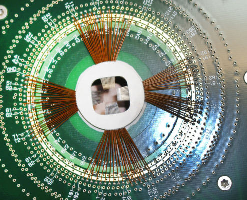
This is where the generic ATE bit stops and the custom per-design bit starts. In order to test a chip on an ATE, you need an interface. If the product requires wafer level testing, then more hardware is needed. In addition to a manual test rig, I will also have been designing a probe card, which will connect to the ATE head with a generic adaptor called a pogo tower.
The interface to the wafer is via a custom-designed circular probe card PCB, which has the matching ring of pogo lands (just surface pads) and a big hole in the middle. The space in the middle is to take the probe ‘spider’ which is a circular array of fine, stiff wires, each with a bend in at the end, terminating in a sharp point. The final shape of this array of points, the probe ‘needles’, is designed to align with the pads on the die, and with some suitable epoxy stiffener spread over the wire array, the probe tips will be perfectly aligned and co-planar. This is a very specialist job to construct and they are delicate assemblies.
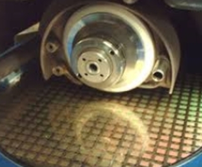
Wafer probers are cool. The idea is you bolt the wafer probe card into the top of the machine, needles-down, then wheel the whole thing over to the ATE. The ATE head will have that pogo-tower already docked. Next you manipulate the test head up, over your head so you can turn it upside down and dock it down onto the top of the wafer prober machine, locking onto the probe card with a twist of a mechanism.
The prober machine will push the wafer up very carefully, into the fixed probe needle array, making all the electrical contacts. It then instructs the tester to test one or more dies and collects the binning results, before stepping onto the next die. This is repeated for the whole wafer, and each wafer in the cassette. The X-Y coordinate of the die and test results are saved to a datalog stream, so wafer maps and yield can be obtained. The wafer map is a lookup table of test result vs die location, and this is what is fed into the assembly line to pick out the good die to package. This used to be done by the machine ink-spotting bad die!
Trouble at t’mill
So that’s the why and how of automated IC test and the development process; back to our story! Our crack debug team consisted of an expert in wafer probers, a mechanical designer, the visiting test floor manager from Philips Semiconductors Calamba (Philippines), and me, then, a test engineer-in-training.
The product was a mature long-running product, built on 200 mm wafers, an older process node (most likely TSMC 350 nm) and was very much just ticking along. Until one day it wasn’t. Wafer probing was courtesy of an old Electroglas EG4080 (pdf of latest 4090 linked) docked up to a Teradyne Catalyst. Quite a common configuration at that time. The yield had dropped to zero, so the first thing they did was to run some correlation wafers that were kept onsite, in a special inert-atmosphere cabinet. These were the same wafers used during development, with all test results kept on file, and used for well, correlation purposes when bringing up a new test stand. They could not get a single die to pass, so we were called in to sort it out.
The Debug
We split up and checked everything. Prober guy checked the EG4080 setup, calibration, looked at it mechanically and inspected the ‘probe marks‘ using the built-in high zoom inspection camera. These witness marks had the characteristic ‘short furrow’ shape, indicating that the needles contacted, then slid slightly across the pad, digging a tiny trench into it. This is because, as the needles made contact, the wafer is driven a little further into the needle, causing it to slide, or scrub laterally. This promotes oxide scrubbing, giving a good electrical contact, and keeps the tips sharp.
There was no evidence of over-driving, or needles deflecting the ‘wrong’ way, and no significant tip wear. Mechanical guy was heavily involved with this process as well as keeping track of tests and checks, and collating all data. I checked the ATE calibration, and inspected all parts of the system, checked that the test program was the correct revision, and initiated a few tests under manual control. I could see which test was failing: pin leakage. Everything else was fine.
This particular test looks for defects in the pad ring, surrounding the die core, or possibly within the package. This works by programming any bidirectional pins to input mode, then sinking a small test current into all input-capable pins, using that PPMU. The results were a bit odd, two pins were giving quite random results, but that was the only obvious fault. We tore it all down again, inspecting every component visually, cleaning contacts, removing dust and contamination, and just looking for any strange current path that could explain what we saw.
The Rogue Beard
Since we couldn’t find anything wrong with the equipment, we started to look at how it was being used. The test floor was typical – climate controlled with a metallised ESD safe floor. All equipment was correctly grounded, all staff fully adorned with overalls, hair coverings and heel grounders. We were just standing around shooting random ideas, talking about contamination and possible environmental factors, when I just blurted out “what if there’s a hair stuck in the probe needles?”
What if there’s a hair stuck in the probe needles?
Pretty much everybody stood there and said that that wasn’t possible, all operators tied hair up under a tight covering, and beards were even covered. “Surely we’d have seen a hair on the cameras?” Nothing was seen. “But, I asked, has anybody actually taken the probe card out and looked at it under a microscope?” “No”, was the answer, as it was delicate, they didn’t want to handle it unnecessarily.
The prober operator just unbolted it and held it up to the light and peered at it closely with a loupe. After a short discussion amongst the floor staff, some tweezers appeared, and the chap very, very carefully pulled out a short, curly ginger hair from between the needles. It went quite quiet on the floor as he proceeded to reassemble the test stack, docked the ATE head, and initiated a manual test on the prober. “Bin 1!” was the exclamation! Switching over to automatic mode, the wafer was probed, and the resulting wafer map on the screen looked exactly like the reference data. Success! The operator in question had a big, ginger beard. We laughed, packed our gear and headed for home. Millions of pounds of electronics equipment, nearly scuppered by a rogue beard hair. You couldn’t make it up.


Nice story! Thanks for writing it up! I’d love to read some more about your chip fab time ;-)
What a great read! While I don’t ever work with anything that delicate, I do find my own beard hairs pretty much on everything I touch. Alas, mine are mostly gray these days.
Great Story. I see lots of engineers who know how to make things work, but it is a different mind set to think about all the ways things might not work. There are several things in this article to file away in the VFOGI (Vast Fund Of General Information)
Thanks for the story. I helped with the building of an In-House designed 2 head ATE many years ago and your story brought back fond memories of the old Test Engineering days and group.
When we’re having continuity and leakage failures, the first thing we do is scrub the pads (our electroglas probers have ceramic scrub pads they can drive the card over to and smoosh it on) and then we start swapping test hardware, probe cards and handler interface boards, specifically because we’ve had a lot of issues with probe tip contamination. (But we’re a remote design center, not a fab, so we have very loose protocol over cleanliness: I’ve had to remove a bit of a doughnut from inside an ATE test head.)
Those electroglas probers are cool, with the prober head a big loose brick of electronics sliding around on a giant two-dimensional linear stepper motor, but they’re kind of a bear to work on.
We’re still recovering from finding that somehow we’d managed to shear two bolts on an older ATE in the prober docking process, so the next time we turned the testhead over preparing to dock it, a bunch of the probe head parts including the pogo tower just fell out. Fun is getting to reassemble a pogo tower with several hundred pogo pins.
So it was hair today, gone tomorrow?
You never said though – were his beard hairs _straight_?
Great story! the troubleshooters basic rules: when things get tough, always return to the basics, and never let someone saying “impossible” stop you from checking something when you’ve run out of “possible”!
Love to see more of these!
Great story! I worked in Semiconductor equipment for many years myself. We had a very rare software bug in a wafer defect
laser scanning machine that took almost a year to track down. A very clever guy on our team finally figured out that a diagnostic message had been lengthened and subsequently overflowed a character buffer and corrupted a flag that caused … very misleading and confusing stuff. Anyway, the ultimate trigger for the problem was that the corrupting message was only ever sent when ZERO defects were found on the wafer. This condition was extremely rare even in the cleanroom production environment, and NEVER encountered on the relatively filthy wafers we had available for software testing.
Great story! I also worked on semiconductor manufacturing equipment and we once had a fiendishly rare bug in a wafer defect scanning machine we produced. After a very long hunt, it turned out that the error occurred only when ZERO defects were detected — something that ALMOST never occurred in a fab and NEVER occurred with the relatively filthy wafers we software engineers had to play with.
Oops, sorry for the double post. My first try didn’t show up for a while.
I have always heard about curl and divergence, but this is the first time it has made sense. The curl of the whisker led to divergence in the test results.
I can show myself out.
Great story, well told. It made for a fascinating and educating read. More of this sort of thing!
Covid lends an idea just how clean is clean and how dirty we are. Skin cells and body hair can cause defects too, even the hair up your nose.
I think there’s an untapped genre of engineering novellas here, like sci fi except interesting
I believe there’s a typo in here: “This is attached viable an umbilical”
Indeed so. Fixed, thanks.
Is there some place where all these “you wouldn’t believe what the problem was” stories are?
These are better than a murder mystery for me!
Try the dailywtf site.
There are some here: https://beza1e1.tuxen.de/lore/
Thanks for the story! Please write more of them on this subject :-)
I’ve got a couple of questions. Firstly, why is the wafer circular? (Is it spun during part of the manufacturing process?)
Secondly, on the picture it seems that the retangular dies are printed right over the edge of the wafer, resulting in only part of the die fitting. Why is this?
Wafers are round b/c that’s the way they’re made.
https://hackaday.com/2020/07/22/jan-czochralski-and-the-silicon-revolution/
But I can’t answer your second question. Maybe it’s just easier to make a square-die mask that’s big enough, and there’s no reason to trim it down to circular?
Optics play a part in the fab process, which I believe is why it’s circular. When it comes to the mask, it’s just tiles being repeated. The further you get from the center of the wafer, the more the process quality will vary.
If you were to look at the wafer under a microscope (or even naked eye sometimes) you can see that the outer ring of the wafer fades away. It’s not a hard cutoff at the edge.
I worked in an R&D fab as a test engineer. I didn’t test the stuff inside the fab though, I tested completed wafers before dicing to see if the designs were actually working. The sort of stuff that happens long before it goes into production. I wish I only had to deal with probe card contamination.
When you start doing semiconductor design at the cutting edge of physics, your options break down. No fun electroglas machines, no ATE systems that work with your technology. We’d try to get quotes for probe cards and the vendors would just respond with a “Thanks, but no thanks” when we sent them the requirements.
Why not design the masks for the wafer diameter being used, so that only full dies are made? Or how about populating the smaller spaces with smaller dies that can be made using the same sequence of steps and materials as the large dies taking up most of the wafer? The smaller dies would have to be aligned so one or two edges match up with the cut lines for the large dies, then their pieces of the wafer would need to be sent to a machine to finish cutting them out, or the cutting machine would need to be automatically adaptable to handle the odd sizes and shapes.
It would be pinching every penny from a wafer, but reducing waste. What’s done with those partial dies from the edges? With all the various materials embedded they couldn’t easily be recycled into making new wafers.
The photo stepper shoots die images across the whole wafer. Like using a spray paint can spraying across and off the edge of a workbench project. It increases robot precision to allow the robot of the photo stepper to move across the wafer in a single direction instead of stopping close to the edge and introduce back lash. At nanometer features incorrect back lash can ruin a whole die row. The partial dies allow for photo registration of the robotics and optics before starting the next row. The partial dies are also often used as a wafer test points in the middle of wafer production runs to verify a production process is done correctly before moving onto to the next part of the die manufacturing process. Shoot, test, develop, test, etch, test, rinse, repeat. Photo, etch and implant registration marks are also used on these partial dies. A complete die is often built in with test points that sacrificial. You can these points on the partial dies for things like testing continuity and break down voltages. That way you do not use up a complete die image for sacrificial die testing. If you are making a wafer full of IC 555 timers it is no big deal. (Except for tight fisted managers and whiney quality control engineers.) It is quite an expensive deal when you are making custom cpu chips and a whole wafer lot of 25 wafers cost over a million bucks. That is when those partial die photo shots come in real handy.
> Secondly, on the picture it seems that the retangular dies are printed right over the edge of the
> wafer, resulting in only part of the die fitting. Why is this?
Essentially it is economics, trying to use every last square millimeter of the wafer.
Each die may contain 10s or 100s of chips, so even a partially exposed shot is going to contain something that can be sold.
The positioning of the shots on the wafer is done to optimise the chip count – normally by shuffling them around in a computer simulation.
There are other limiting factors, the tilt of the wafer surface is measured in each shot by (in the simplest case) 5 focus channels arranged as in the 5 points on a dice – for a succesful measurement, at least 3 need to be on the wafer.
In addition, some empty space on the corners is needed for alignment marks for the ‘back end’ machines that to things like wafer test or sawing.
In addition to all this, there is an unusable ring at the edge of the wafer due to process effects that needs to be taken into account.
wafer is circular being a slice of a silicon ingot which is a cilinder (and that is due to the way it gets grown to allow the wanted regulat lattice geometry. Some dies are half formed at the edge of the wafer ad the reticle (that is the ‘stamp’ that gats repeated to cover the wafer in manufacture phase) contains several dies not a single one.
I love these war stories, please have more on HaD it’s a delight.
[quote] gold (or copper, lately) bond wires are attached between this leadframe and the chip pads, using a wire-bonder machine[/quote]
Does replacing gold with copper implies new risks? Won’t it makes chips fail down the line in a few years akin the whole RoHS fiasco did by enabling tin whiskers growth?
Also I’m very happy to finally see an [img=https://hackaday.com/wp-content/uploads/2022/01/WaferDice2.jpg]actual die saw[/img] pictured in this article since in all the videos and book on IC fabrication (from sand to chips) this step is either crudely drawn or entirely skipped! I for one would love to read/see more about this crucial step (how such precise saws are made, how they operate etc…)
The switch to copper started almost 20 years ago so the bugs have been largely worked out. All but the most anal users (some in the defense industry where I work) now accept that copper bond wires ate as good as gold. There was a significant learning curve and lots of papers 10 – 15 years ago about newly discovered solutions to issues with copper wire bonding. Automobile electronics must tolerate harsh environments; lots of temperature cycling and physical vibration. Initial copper bonding processes started off using the same parameters that worked for gold. Copper is harder than gold and the force of the molten copper ball impacting and solidifying on the pads caused cracks more often than gold; all other things being equal. Cracked pads often function fine until thermal cycling and physical vibration make the cracks worse over time. Also the halogen containing encapsulation material used for packaging 10+ years ago caused slow corrosive degradation of copper bond wires particularly in high humidity environments. Modern bonding processes that account for copper’s hardness and other physical parameters along with low or zero halogen encapsulation resins have rendered copper bonds as reliable as gold despite paranoia among certain ex auto industry types now in aerospace and defense who got burned back in the day and can’t let it go. Even NASA has blessed copper bond wire use in high reliability space systems although the recommend more extensive QC testing and qualification.
Copper conducts both heat and electricity better than gold, is physically stronger and cheaper; although cost difference between gold and copper high purity 50 micron bond wire is nowhere near the raw material cost difference. From an engineering performance standpoint copper rules. The only drawbacks, need for tighter process control to prevent pad cracking and corrosion due to halogens in encapsulation resin, are readily manageable. The change from gold to copper is inevitable for most ICs and some manufacturers, TI for example, are phasing out gold wire bonds completely.
Max L.
Thank you for you very thorough and instructive answer. I come on HaD for these kind of interaction with knowledgeable people like you.
So this is kind of off-topic but kind of not. Do you know whom (or at least what “kind” of company) would be appropriate to contact to get wafers packaged, specifically in DIP28? I have access to wafers of a chip I need but the company that manufactures the silicon no longer wants to manufacture it in DIP28 package. I’d love to get 100,000 or so chips but I couldn’t figure out how to make it happen. Any thoughts?
It’s been too long, and the local prototyping house I’ve seen used on my projects is long gone. But you could start at ASE Group: https://ase.aseglobal.com/en/products/assembly_offerings/leadframe_solution
Who still seem to offer PDIP. I’ll ask around see what I can find, but my answers will likely be UK-specific.
Rochester Electronics and Micross are the only companies that would give us the time of day when we needed a specialty packaging of bare die for my company.
Oh yeah, it won’t be cheap. I have limited experience with small volume IC’s (100k is probably small to medium volume) but I doubt anyone can do it for $10 a piece and it can easily become a multiple of that depending on the availability of the package, new versus existing tooling and the level of testing. No test and they are not responsible for any failures. Simple connection test will only check the impedance of the pins to verify connection to the die. Full parametric testing can be well into 6 digit engineering cost depending on the complexity of the part.
They will want to run it all at once, so you are probably looking at a 7 figure investment.
Depending on the application it might be cheaper to do bare-die on board (glop-top) or buy a smaller package version of the part and create a small FR4 with through hole pins in the appropriate location to fit into a DIP footprint on a board. The cost will probably still be high, but there will be more options for smaller runs so there won’t be a multi-million dollar investment.
Forgive me for going on too long… your problem is more interesting than the work I’m supposed to be doing.
You are most welcome.
Love this story. Many war stories of fab life like this one. Once a fab rat, always a fab rat.
Thanks for the story! I designed some of the instrument calibration for the Catalyst, fun times!
For developing and troubleshooting the instruments, we had special test-beds, which allowed us full access to both sides of the 16×20 inch circuit boards. When working on them, we needed to be careful to remove any jewlery… the 3.3v power supply would not shock you, but the 400A behind it could probably melt a ring. Sometimes an instrument prototype would misbehave, only to function perfectly once an oscilloscope probe was attached (presumably due to parasitic capacitance of the probe); in response to that frustration, we would joke that perhaps we should tweak the design and ship the scope probe as part of the instrument.
Sounds familiar. I worked as a PCM test engineer for many years. As soon as pin leakage failures were mentioned, I thought, ” There’s a piece of lint or a hair stuck somewhere”. The alternative was that someone had touched something without gloves on. Even the small amount of moisture and oil from a fingerprint can throw off measurements if you’re limits are in picoamps.
Been doing DFT for 20+ years.
I done every type of scan from MUX-DFF to LSSD.
TetraMAX is a terrible tool, so is DFT-Compiler.
BSD-Compiler is not terrible.
Latches are only your friend when crossing clock domains.
Never-Ever trust the ATE Setup.
Never-Ever trust the ATE.
Simulate early, simulate often.
Never-Ever trust CTL models, especially from vendors.
Never-Ever trust the tech libraries.
Never-Ever trust the STA team.
set_test_assume is an evil command and should never be trusted.
Synopsys OCC controllers are terrible.
Synopsys Compressors [non serializing] are terrible.
The Documentation is always crappy.
Never Ever trust the Analog Group.
PLLs are evil and will break your simulation.
EFUSEs are a PITA.
Always verify Memory BIST WITH a FAILURE.
ATPG isn’t.
The customer is always an idiot.
“Pushbutton” flows are not.
Oh, I hear you loud and clear. I’ve been a test engineer, and an digital IC designer, specialising in test and DFT. Thing is, you’re stuck with the flows your company has bought into, or the project lead is comfortable with, despite the, er, issues you allude to. The mantra of “trust nothing, verify everything” is something to cling onto until your last breath. The list above is just the tip of the iceberg. I have many, many stories of pain and suffering in IC design and test!
The in-process quality controls are very interesting. But the failure is really prosaic. it’s right up there with damp electrodes and swarf in grease.
But thanks for summarising the process.
The only thing the author ignored is “simple reasons first” paradigm which our debuggers use. Would cut much of the disassembly and tsting time in this case.