There was a time when all that was available to the electronics hobbyist were passive components and vacuum tubes. Then along comes the integrated circuit, and it changed everything. Fast forward a bit, and affordable programmable microcontrollers arrived on the scene. Getting started in electronics became far easier, and the line between hardware and software started to blur. Much more recently, the hobbyist community was introduced to field programmable gate arrays (FPGAs) and the tools necessary to work with them. While not as widely applicable as the IC or MCU, the proliferation of FPGAs among hardware hackers once again opened doors that were previously locked tight.
We’re currently on the edge of another paradigm shift, but it’s no surprise if you haven’t heard of it. After all, the last couple of years have been a bit unusual, so the 2020 announcement that Google was teaming up with SkyWater and Efabless to enable the design and manufacture of open source application-specific integrated circuits (ASICs) flew under the radar for many people. But not Matt Venn, the host of this week’s Hack Chat. For him, it was the opportunity he’d been waiting for.
 Matt started like many of us, building electronic kits and building new gadgets out of old discarded hardware. He graduated to microcontrollers, and became particularly interested in FPGAs when the open source toolchains started hitting the scene. Of course by this point, it was much more than just a hobby for him. He was presenting a talk at the 2019 Week of Open Source Hardware in Switzerland when he saw Tim Edwards from Efabless demo a chip that had been made with open source tools. Unfortunately, the costs involved were still far too high for an individual to put their ideas into silicon.
So when Google and Skywater announced they would be footing the bill to have selected open source ASIC designs manufactured a few months later, Matt says he was in a good position to jump in. He has since started running the Zero to ASIC Course which aims to teach you how to produce your own chips using the open source Process Development Kit, and so far 160 people have taken him up on the offer.
As you might expect, many of the questions in the Chat had to do with what kind of designs you can actually produce using the 130 nm process. Especially given the limits on the physical space each creator’s circuit can take up on each multi-project wafer (MPW). Others wanted to know how difficult it would be to port over existing FPGA designs, or how well the process worked with analog applications. With the number of designs Matt has seen go through his course, he could answer many of the questions just by pointing to a particular individual’s ASIC. For instance, he held up the digital-to-analog converter from Harald Pretl and Thomas Parry’s 5 GHz satellite transceiver as prime analog examples.
So let’s say you put the work in to design an ASIC and it gets approved to be produced on a future MPW, what then? Well, first you have to hope everything goes according to plan. Matt explains that the initial run was almost a total write-off due to timing problems in the toolchain, though in the end, he was largely able to recover his own chip. But they’ve done several runs since then, so let’s assume there’s no production problems. What exactly ends up on your doorstep?
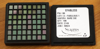
If you were expecting a handy DIP8, you might be disappointed. While some DIY friendly packages would be nice, right now the ASICs ship as wafer level chip scale package (WLCSP) with an unforgiving 0.5 mm pitch. If you can believe it, that’s actually an improvement over the first run, which shipped out as a bare die. Of course as Matt pointed out, anyone who’s gotten to the point of designing their own custom ASIC probably won’t be scared off by the prospect of some fine-pitch soldering. Some in the Chat wondered about the difficulty in getting compatible PCBs produced, but Matt said that in his experience OSH Park has been up to the challenge.
Like the Metal 3D Printing Hack Chat before it, this week’s session went over a topic that’s on the absolute cutting edge of what’s possible for hardware hackers and hobbyists. Truth be told, the vast majority of the people reading Hackaday are no more likely to send away for their own custom ASIC as they are to battle x-rays in an attempt to sinter metal with a homebrew electron gun. But that doesn’t make the fact that some folks out there doing it any less important, or inspiring. That said, if you do end up being one of those select few that can boast they’ve designed a custom chip of their own — don’t forget to send one of them our way.
We’re grateful Matt Venn was able, once again, to share his valuable experience in the realm of open source application-specific integrated circuits with us. If you haven’t checked them out already, the Zero to ASIC workshop he ran for Remoticon 2020 and his talk Open Source ASICs – A Year in Perspective from Remoticon 2021 are required viewing if you want to learn more about this fascinating new frontier in hardware hacking.
The Hack Chat is a weekly online chat session hosted by leading experts from all corners of the hardware hacking universe. It’s a great way for hackers connect in a fun and informal way, but if you can’t make it live, these overview posts as well as the transcripts posted to Hackaday.io make sure you don’t miss out.


There’s lots of excellent stuff in Matt Venn’s interviews and they keep getting better and better. His interview with Thomas Parry and https://github.com/yrrapt/analogue_design_example is pure and solid gold.
Thanks Ethan!
Thanks for the write-up! One small correction: mpw1 shipped with both bumped dies ready for pcb and bare dies. For future runs we are only expecting bumped dies.
Really love to see a maskless 1-2um process that would let you target something like 30mm^2 inside a standard package and IO bond pad layout with whatever you want. Would open up small ASIC design like the internet PCB companies did 20 years ago.