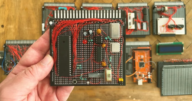
While the phrase “I built my own computer” might sound impressive to the uninitiated, anyone with an interest in modern computer hardware knows that there’s really not much to it: buy a case, a motherboard with a CPU, some RAM and peripherals, and you’re pretty much there. What’s way more impressive is designing a complete computer system from the ground up, as [Joshua Coleman] just did when he built the Coleman Z80.
And when we say “from the ground up”, we mean it: everything down to the system bus was hand-drawn by [Joshua] himself. It does share something with modern PCs though: a strictly modular design. There’s a Z80 CPU board, a ROM and RAM board, and even two modules that you could describe as a video card and a sound card. All of these are built on prototyping boards with a 40-pin edge connector and hooked up to a single backplane carrying the main system bus.
Designed as an experimentation platform, the Coleman Z80 has many features that enable testing and debugging, such as an adjustable clock generator and a few beautiful vintage LED displays that show the status of the main bus. Input and output are mainly through a serial link and a 16×2 LCD, but [Joshua] is already planning a keyboard interface and composite video output to give it that proper 1980s home computer vibe. The software is currently limited to a ROM monitor that enables basic I/O commands, but with 256 KB of RAM there’s plenty of potential for writing useful software.
Just as impressive as the design itself is the fact that this was [Joshua]’s first electronic design project; we’ve certainly seen worse first projects! Over the years we’ve featured several cool homebrew Z80 computers, such as a super-minimalistic board, a modular system based on the powerful eZ80, and this cute little one that fits inside an Altoids tin.


This brings back memories. My first from the ground up was an 8008, I had to build everything. Next computer was a z80 cpm based computer built not quite from ground up but almost. But I never want to go back to this, it is a lot of work. Congrats on the build.
Thank for this,
Hearing from someone that was there that “The old ways” weren’t the best it’s refreshing, I spent too much time with “Classic Engineers” and people thinking that the ’80s were like synthwave videos recently.
As it could be satisfying to do such archivement we should totally understand the practicality of it.
Absolutely. Been there. I built a lot of stuff for medical research in the 1980s using 6502, Z80 and 8086 processors and several different bus architectures, also DEC Unibus. Hardware that took days to build and then code in assembly, I could do now with just code on an Arduino in a few hours. Not to mention it will run off a 9 Volt battery instead of a 72 inch rack on 3-phase 208 vac at 15 amps.
No, I don’t pine for the old days.
Everything was fine, until you moved forward. I was satisfied with the 6502 until I moved to the 6809. Cassettes were great for saving files, until I got m my first floppy. Floppies were fine until I got my first hard drive.
Though, I got a C compiler in 1988, and never really used it. At 1 or 2MHz clock, and two floppy drives, it was just too much trouble.
Yeah! I’m a lot younger than a lot of people here, at 15, and I don’t think we need to go back to the 80s, but retro tech is super cool.
Hey there! This is my build and you’re right a lot of work! My personal goal is to understand FPGA which is apparently an infinitely configurable amount of transistors which can emulate anything. But, to get there I felt going through this hard work and ground-up design was necessary. I would love to work in hardware engineering or peripheral to it despite not having a degree in computer science. But, these days all the FPGA stuff and crazy advancements are baffling to me in regards to implementation. I think I’m on my way!
As an aside, what grinds my gears though is how much harder it is to crack into the scene of employment with merely a little interest and a sparkle in the eye like so many Baby Boomer employment stories go lolol. “Yeah so I just asked this guy with an oscilloscope what he was doing and I ended up lead engineer at Commodore!” Oh how I wish! Alas, off to LinkedIn I go….
Even with the CE/EE background it’s intimidating, thanks to the wonder that is military personnel assignments i’ve spent my service time essentially doing IT management for .gov. Now spend evenings and weekends tinkering and building the knowledge to pursue my passion ( DSP, including doing some algoritms on fpga fabric). Keep it up very impressed with your build.
Thanks for the encouragement friend.
Building with old school discrete ‘VLSI’ like this will give you some sense of what to do in an FPGA, you are correct in general about that .. but there is one pretty serious difference you’ll hit when you make the jump. When I first ventured into FPGA-land, after having built a couple 8 bit SBCs (6809, z80), the first thing that hit me was “where are my three-states? Where are the Hi-Z capable elements?” I was very used to thinking in terms of chip selects and using tri-state devices bussed together, and could find none of this in the FPGA environment. When you get there you have to start thinking more like multiplexing. Turns out the old select-one-device to drive the bus, everybody else is Hi-Z, is just a way to build a multiplexor, assembled from independent parts. Well, inside the FPGA, there are no independent parts, the whole design is in-house as it were, so you’ll find yourself crafting these beastly multiplexor-looking things. It felt ugly at first, like being forced to add these extra parts I shouldn’t need, but after a while, it still felt ugly. But I guess you get used to it.
wow man thanks so much for that really down-to-earth sneak peak. i fully understand what you have said and that has actually tantalized me lolol. any good links for first approach to DIY FPGA learnings? thanks!
Not the OP but I started following along with Ben eaters 8bit computer tutorial and then learning how to make the individual parts in verilog and then add them all together, I used a lattice Mach X02 and most of my computer was built using their IP blocks (essentially pre made configurable blocks that let you use parts of the board like RAM or DSP elements easier), although for some basic things like adders you don’t have to use IP blocks if you don’t want too.
The thing that tripped me up a bit with that, as has already been mentioned, is the need to multiplex the busses, it’s really not that bad though, you just need a switch case statement, essentially if control signal is 0 then bus = signal0, etc. It probably is more compact doing it on an FPGA with a multiplexer than using chip selects. Your control signal rather than having a one hot assignment, you can just use binary numbers, so greatly reducing the number of control bits you need. I am learning vhdl for university now, so I think it’s about time I attempt to build another computer.
If you are looking for FPGA boards, obviously I’d recommend any of the big companies development boards, but they can get expensive very fast, if you want something a bit cheaper then the sipeed tang series are very good, not much documentation but you don’t really need much for an FPGA, you will need your own switches, seven segment displays etc though because the boards don’t come with any. If you are feeling extra brave then there are decommissioned bitcoin mining control boards that have a xilinx zynq 7010 on them, that’s 2 arm A something cores and an FPGA only for about £12, they are called ebaz4205 I think, they are much more difficult to set up and you need a JTAG programmer but could be very powerful.
I don’t know if you are into games at all, but a game on Steam called Turing Complete is very good, essentially starting with building basic digital logic components and building them up until you have a full CPU that you run assembly code on, if nothing else for me it’s fun whilst providing some challenge at times.
I have taught Digital Circuits, an undergrad logic course. I have the students suffer though a couple of labs with real TTL MSI scale parts and then translate the labs into FPGA implementations using Terasic’s very affordable DE-10 Lite board (Altera Max 10 FPGA). I have them code a sequence generator in VHDL and integrate it with schematic capture using virtual TTL in Quartus Prime. I would have given the proverbial eye teeth to have a cheap powerful board like the DE-10 Lite and an FPGA IDE such as Quartus back in the 1980s. Engineering productivity can be off the charts now compared to back then.
Inside the FPGA sure there is no Tri-state HiZ but you have an abundance of interconnect wires to allow separate buses, and logic read/write/select states. You can have have your own bus to local memory, another dedicated bus to another component that 30 years ago was attached electrically through the PCB. While EE architecture of 8 bit CPUs worked this way, even the modern PC has separate electrical busses now to increase data paths to performance critical components PCIe, DDR.
But on the outside of the FPGA you do have HiZ electrically on the Output Buffers, as many FPGA allow many pins to be bidirectional, but this depends on exact FPGA you choose.
My first computer had its beginning when I bought an 8080A from Radio Shack, plus three or four prototype boards and edge connectors. The CPU board included an octal address & data display, an 8-position dipswitch and a pushbutton. The memory board had 1K of static RAM. The backplane was built into the chassis of an old Heathkit vacuum tube stereo amplifier. I programmed it by setting the dipswitches to an 8-bit value, then pushing the button to store the byte in memory and advance to the next address. Each byte took at least 30 seconds to program and errors were common.
I migrated all the electronics to an S-100 bus prototype board, added a keyboard and TV display interface, programmed a primitive operating system into a 1K byte EEPROM, and kluged a circuit to store data on audio cassettes. The Heathkit chassis was reborn as an analog power supply sufficient to heat a small apartment.
Gawd, those were the days.
congrats on doing this. you did have to work hard for so very little.
That reminds me of the NDR Klein Computer. (https://en.wikipedia.org/wiki/NDR-Klein-Computer) I always wanted to build it, but I think I was simply to young back then.
My first job out of school was at Data General. My first project (there were four? of us) was a low cost “glass Teletype” terminal, built around the Motorola 6802. It was a perfect first project. I ended up working on the keyboard, which was capacitive, and built totally from scratch. We designed the whole thing: PCB, keys and support structure, enclosure, and assembly code to drive it (there was no micro in the keyboard as is common today). The goal was a sub $300(?) cost terminal, so there was a cheap feel to it, but it replaced a terminal that cost DG thousands to make.
Anyway, one of the tasks I had was to life test the keyboard. To do that, I ordered a couple of MEK6800D2 eval kits, parts of which I still have in my attic. Think KIM-1 but with a 6800 instead of a 6502. And a bit more versatile — they had a breadboarding area and a UART. You could order a MIKBUG PROM and upgrade them from keyboard interface to serial interface, which is what we did. You could also add user code EPROMs, which we also did. The modified eval boards tested and recorded the keyboard performance.
So, for a beginning engineer, this was a perfect introduction to the 6802 (also, EPROMS, serial and parallel IO, memory maps, etc). Not surprisingly, there were also plenty of “extra” 6802 chips lying around the lab, some of which got grabbed and built into a repeater controller for the DG ham radio club (by me). I also wrote the control code for the display keyboard and for the repeater controller, all in assembly. I did many other 6802-based controllers in later years, mostly wire-wrapped, because I had all the tools and at DG we prototyped on wire-wrap boards, which could be stripped and re-used for personal projects after the DG project was over.
I love old war stories like this, thank you
That brings back memories doing wire wrap. If done properly, wire wrap can last. I recently ran across a gadget I built around a 6502 and 6522 VIA which I built about 35 years ago. I plugged it in and it fired right up.
I built the project to monitor the serial cons of an AT&T 3B1 which used a Telebit 23K bit/S to talk to LLNL by UUCP for e-mail and Usenet traffic. My device operated a soldid state relay to power cycle the 3B1 if no serial activity was detected for five minutes. Status was displayed on a 16 character LCD – same protocol as is still popular on Arduino, etc. I had a 2K byte 6116 static RAM and a 2K byte 2716 EEPROM. I coded my program on a PC-AT using TASM cross assembler to generate a HEX file which was then burned into the 2716 with an AT bus programmer from JDR Microdevices.
You could do it quite easily on a PIC now, or save time using a ready to drop in Arduino.
What you could cobble together with a RadioShack wire wrapping tool!
The computer store guy who showed me how to decode addresses with a 74LS138, was a God to me, when I was 15!
Oh, the ‘138, wonderful little glue chip! All my 8 bit designs had one or two to create the memory map. At least, until the PAL/PLA/GAL/CPLD thing started happening.
I’ve still got my RS wire wrapping tool. The real miracle is that it still has the little wire stripper that goes inside.
Same!
My first co-op job was fixing a board with about 50 CMOS 4000 series chips which RCA made as a one-off for the US Army. The person(s) who built it followed the schematic correctly but used slit-n-wrap. I learned to curse that stuff, which unless the gun were held perfectly makes the wire wrapping equivalent of a cold solder joint. A lot of the wraps were three level and seemed like more often than not the bad wrap was on the bottom! I wound up redoing the board with an OK tools 120 Volt gun and precut wire. After I was done, I didn’t hear back, so I assume it worked for whatever it’s intended mission was.
When I was 15 I designed and (mostly) completed building a z80 “handheld” in a form factor similar to the Newbury Newbrain, about 10″ wide and 4″ high.
As I recall it would have had 2k ram as 4x 2114 chips and a 2732 8k eprom. Zilog CTC and SIO chips filled out the I/O. A cassette interface connected to the SIO was based around published designs, but not built. Plans for a keyboard & one line 16 char 14 segment led display (which I couldn’t afford (!)) would have been the user interface. Power would have been 4x AA batteries, though I didn’t solve how to regulate that voltage as the lm7805 needed more voltage difference than that.
The main board was built on prototyping board and wired with a ‘pen’ that delivered fine blue plastic coated wire down the centre from a spool. A sharp edge at the nib-end meant you could cut the wire by pressing against the pcb. I dont remember what it was called.
I built a case, too, using plasticard and solvent glue, but it was rather weak and hasn’t lasted.
It wasn’t finished because I had too little support or kit available … this was truly bedroom build with a multimeter and an antec 25w iron. I still have the incomplete build though, and the multimeter. :)
Reminds me of the Sega G80 system; a modular board system with six slot edge connector backplaned cardcage. Swapping boards out would make different games:
z80 CPU board with memory
Display boards (either vector monitor or raster monitor boards)
Ssound boards (at least 5 different kinds, including a speech board)
ROM board
Using a mix and match would create many of their early 80’s arcade games with different capabilities.
I didn’t see the appeal of those single board Z80 computers, I was more interested in complete systems like the MSX at the time lol! I’m now considering designing and building an MSX computer of my own. Something like the Omega project but with more synth chips and modern MCU as a coprocessor. Could be a nice platform for experimentation.
The Altair 8800 was just a complicated “single board computer” until you added enough boards to make it useful.
The KIM-1 was a lot more viable, until you added ots of boards to make it much fancier.
A single board computer got you going, it took less work and cost less.
There’s also a spread. In 1975, a simple computer meant more than in the days of consumer computers. By then “bigger” systems” more more available, and cheaper.
Imagine, just having a thing with some registers and 128 bytes of RAM and a couple of stylin’ red LEDs *at*home*, when the other hottest tec the average person could lay hands on was CB radio or a pocket calculator. It was a far cry from anything you’d call a computer now, but it was Mad Scientist stuff at the time
If this chip drought doesn’t let up, we’ll all be reduced to this.
It’s not the worst thing in the world. Building a micro with a firmware monitor and programming it in assembly (or hex from the keyboard) is an excellent way to learn the basics of design and micro architecture.
I’m not saying, build your own chips, but it’s pretty easy to get a Z80 or whatever and add memory, write a monitor and build a keyboard/display I/O. When I built my 6802 projects, Motorola had a wealth of applications publications that walked you through the whole process. The MEK6800D2 kits had complete documentation, including schematics and BOM, so it was easy to start from that baseline and add and subtract to get what you needed.
The two monitor ROMs, JBUG (I think) for the keyboard/display and MIKBUG for the serial interface, were also completely open, you could even get the code on tape from Motorola, so you didn’t have to type it in and compile it (we bought a MIKBUG ROM and dumped it, then copied the hex into an EPROM. I do not miss the old DATA I/O programmers and their silly hex chip ID codes that you had to look up before you could program a chip.
And there were a bunch of variant Bug monitors that were plugin. They’d keep the important entry points in the same place, but add features.
Enter the Omega Delta System…
The ODS was developed in the early 1980’s. It was an answer to the process of upgrading a computer of processor(s), memory or other functions current or future. The system was capable of incorporating new processors among older processors. New memory technology to old. New functionality to old.
To add ability to a OD system, it was as simple as adding a card. The proto system was based off the IEEE-696 buss (previous S-100), this buss offered:
• Buss request collision detection and resolution
• Buss expansion, within reason
• Daughter card indexing, needed for redundancy and shadowing
There were several other key developments that were required:
• Addressing scheme, unlimited storage capacity
• Instructions for a functional programming system
• Control the level of a functional buss to provide a mix of functions accomplished by hardware or software
• Unlimited memory capacity, short duration (monolithic) or long term (disk), or any other architecture
• Interfacing different processor technologies and architecture concurrently
• New data storage representations
• New programming language to allow synchronous and asynchronous tasks known as threads today
• Virtual machine, host and guests
• Virtual storage (memory), aka., paging
• Many others
The initial proto utilized the 6502 and its companion chips. Various other functions of various technologies were added to test its flexibility. It was quite a project.
I wondered when another would approach the ODS concept.
For other possibilities of your project, look into the Rockwell AIM 65.
Much luck on your endeavors.